


User’s Manual
All information contained in these materials, including products and product specifications,
represents information on the product at the time of publication and is subject to change by
Renesas Electronics Corp. without notice. Please review the latest information published by
Renesas Electronics Corp. through various means, including the Renesas Electronics Corp.
website (http://www.renesas.com).
RL78/G13
User’s Manual: Hardware
Rev.3.40 May2018
16
16-Bit Single-Chip Microcontrollers
www.renesas.com

Notice
1. Descriptions of circuits, software and other related information in this document are provided only to illustrate the operati
on of
semiconductor products and application examples. You are fully responsible for the incorporation or any other use of the circuits,
software, and information in the design of your product or system. Renesas Electronics disclaims any and all liability for any losses and
damages incurred by you or third parties arising from the use of these circuits, software, or information.
2. Renesas Electronics hereby expressly disclaims any warranties against and liability for infringement or any other claims involving patents,
copyrights, or other intellectual property rights of third parties, by or arising from the use of Renesas Electronics products or technical
information described in this document, including but not limited to, the product data, drawings, charts, programs, algorithms, and
application examples.
3. No license, express, implied or otherwise, is granted hereby under any patents, copyrights or other intellectual property rights of Renesas
Electronics or others.
4. You shall not alter, modify, copy, or reverse engineer any Renesas Electronics product, whether in whole or in part. Renesas Electronics
disclaims any and all liability for any losses or damages incurred by you or third parties arising from such alteration, modification,
copying or reverse engineering.
5. Renesas Electronics products are classified according to the following two quality grades: “Standard” and “High Quality”. The intended
applications for each Renesas Electronics product depends on the product’s quality grade, as indicated below.
“Standard”: Computers; office equipment; communications equipment; test and measurement equipment; audio and visual equipment;
home electronic appliances; machine tools; personal electronic equipment; industrial robots; etc.
“High Quality”: Transportation equipment (automobiles, trains, ships, etc.); traffic control (traffic lights); large-scale communication
equipment; key financial terminal systems; safety control equipment; etc.
Unless expressly designated as a high reliability product or a product for harsh environments in a Renesas Electronics data sheet or other
Renesas Electronics document, Renesas Electronics products are not intended or authorized for use in products or systems that may pose a
direct threat to human life or bodily injury (artificial life support devices or systems; surgical implantations; etc.), or may cause serious
property damage (space system; undersea repeaters; nuclear power control systems; aircraft control systems; key plant systems; military
equipment; etc.). Renesas Electronics disclaims any and all liability for any damages or losses incurred by you or any third parties arising
from the use of any Renesas Electronics product that is inconsistent with any Renesas Electronics data sheet, user’s manual or other
Renesas Electronics document.
6. When using Renesas Electronics products, refer to the latest product information (data sheets, user’s manuals, application notes, “General
Notes for Handling and Using Semiconductor Devices” in the reliability handbook, etc.), and ensure that usage conditions are within the
ranges specified by Renesas Electronics with respect to maximum ratings, operating power supply voltage range, heat dissipation
characteristics, installation, etc. Renesas Electronics disclaims any and all liability for any malfunctions, failure or accident arising out of
the use of Renesas Electronics products outside of such specified ranges.
7. Although Renesas Electronics endeavors to improve the quality and reliability of Renesas Electronics products, semiconductor products
have specific characteristics, such as the occurrence of failure at a certain rate and malfunctions under certain use conditions. Unless
designated as a high reliability product or a product for harsh environments in a Renesas Electronics data sheet or other Renesas
Electronics document, Renesas Electronics products are not subject to radiation resistance design. You are responsible for implementing
safety measures to guard against the possibility of bodily injury, injury or damage caused by fire, and/or danger to the public in the event
of a failure or malfunction of Renesas Electronics products, such as safety design for hardware and software, including but not limited to
redundancy, fire control and malfunction prevention, appropriate treatment for aging degradation or any other appropriate measures.
Because the evaluation of microcomputer software alone is very difficult and impractical, you are responsible for evaluating the safety of
the final products or systems manufactured by you.
8. Please contact a Renesas Electronics sales office for details as to environmental matters such as the environmental compatibility of each
Renesas Electronics product. You are responsible for carefully and sufficiently investigating applicable laws and regulations that regulate
the inclusion or use of controlled substances, including without limitation, the EU RoHS Directive, and using Renesas Electronics
products in compliance with all these applicable laws and regulations. Renesas Electronics disclaims any and all liability for damages or
losses occurring as a result of your noncompliance with applicable laws and regulations.
9. Renesas Electronics products and technologies shall not be used for or incorporated into any products or systems whose manufacture, use,
or sale is prohibited under any applicable domestic or foreign laws or regulations. You shall comply with any applicable export control
laws and regulations promulgated and administered by the governments of any countries asserting jurisdiction over the parties or
transactions.
10. It is the responsibility of the buyer or distributor of Renesas Electronics products, or any other party who distributes, disposes of, or
otherwise sells or transfers the product to a third party, to notify such third party in advance of the contents and conditions set forth in this
document.
11. This document shall not be reprinted, reproduced or duplicated in any form, in whole or in part, without prior written consent of Renesas
Electronics.
12. Please contact a Renesas Electronics sales office if you have any questions regarding the information contained in this document or
Renesas Electronics products.
(Note 1) “Renesas Electronics” as used in this document means Renesas Electronics Corporation and also includes its directly or indirectly
controlled subsidiaries.
(Note 2) “Renesas Electronics product(s)” means any product developed or manufactured by or for Renesas Electronics.
(Rev.4.0-1 November 2017)

NOTES FOR CMOS DEVICES
(1) VOLTAGE APPLICATION WAVEFORM AT INPUT PIN: Waveform distortion due to input noise or a
reflected wave may cause malfunction. If the input of the CMOS device stays in the area between VIL
(MAX) and VIH (MIN) due to noise, etc., the device may malfunction. Take care to prevent chattering noise
from entering the device when the input level is fixed, and also in the transition period when the input level
passes through the area between VIL (MAX) and VIH (MIN).
(2) HANDLING OF UNUSED INPUT PINS: Unconnected CMOS device inputs can be cause of malfunction. If
an input pin is unconnected, it is possible that an internal input level may be generated due to noise, etc.,
causing malfunction. CMOS devices behave differently than Bipolar or NMOS devices. Input levels of
CMOS devices must be fixed high or low by using pull-up or pull-down circuitry. Each unused pin should be
connected to VDD or GND via a resistor if there is a possibility that it will be an output pin. All handling
related to unused pins must be judged separately for each device and according to related specifications
governing the device.
(3) PRECAUTION AGAINST ESD: A strong electric field, when exposed to a MOS device, can cause
destruction of the gate oxide and ultimately degrade the device operation. Steps must be taken to stop
generation of static electricity as much as possible, and quickly dissipate it when it has occurred.
Environmental control must be adequate. When it is dry, a humidifier should be used. It is recommended
to avoid using insulators that easily build up static electricity. Semiconductor devices must be stored and
transported in an anti-static container, static shielding bag or conductive material. All test and measurement
tools including work benches and floors should be grounded. The operator should be grounded using a wrist
strap. Semiconductor devices must not be touched with bare hands. Similar precautions need to be taken
for PW boards with mounted semiconductor devices.
(4) STATUS BEFORE INITIALIZATION: Power-on does not necessarily define the initial status of a MOS
device. Immediately after the power source is turned ON, devices with reset functions have not yet been
initialized. Hence, power-on does not guarantee output pin levels, I/O settings or contents of registers. A
device is not initialized until the reset signal is received. A reset operation must be executed immediately
after power-on for devices with reset functions.
(5) POWER ON/OFF SEQUENCE: In the case of a device that uses different power supplies for the internal
operation and external interface, as a rule, switch on the external power supply after switching on the internal
power supply. When switching the power supply off, as a rule, switch off the external power supply and then
the internal power supply. Use of the reverse power on/off sequences may result in the application of an
overvoltage to the internal elements of the device, causing malfunction and degradation of internal elements
due to the passage of an abnormal current. The correct power on/off sequence must be judged separately
for each device and according to related specifications governing the device.
(6) INPUT OF SIGNAL DURING POWER OFF STATE : Do not input signals or an I/O pull-up power supply
while the device is not powered. The current injection that results from input of such a signal or I/O pull-up
power supply may cause malfunction and the abnormal current that passes in the device at this time may
cause degradation of internal elements. Input of signals during the power off state must be judged
separately for each device and according to related specifications governing the device.
How to Use This Manual
Readers This manual is intended for user engineers who wish to understand the functions of the
RL78/G13 and design and develop application systems and programs for these devices.
The target products are as follows.
● 20-pin: R5F1006x (x = A, C, D, E)
R5F1016x (x = A, C, D, E)
● 24-pin: R5F1007x (x = A, C, D, E)
R5F1017x (x = A, C, D, E)
● 25-pin: R5F1008x (x = A, C, D, E)
R5F1018x (x = A, C, D, E)
● 30-pin: R5F100Ax (x = A, C, D, E, F, G)
R5F101Ax (x = A, C, D, E, F, G)
● 32-pin: R5F100Bx (x = A, C, D, E, F, G)
R5F101Bx (x = A, C, D, E, F, G)
● 36-pin: R5F100Cx (x = A, C, D, E, F, G)
R5F101Cx (x = A, C, D, E, F, G)
● 40-pin: R5F100Ex (x = A, C, D, E, F, G, H)
R5F101Ex (x = A, C, D, E, F, G, H)
● 44-pin: R5F100Fx (x = A, C, D, E, F, G, H, J, K, L)
R5F101Fx (x = A, C, D, E, F, G, H, J, K, L)
● 48-pin: R5F100Gx (x = A, C, D, E, F, G, H, J, K, L)
R5F101Gx (x = A, C, D, E, F, G, H, J, K, L)
● 52-pin: R5F100Jx (x = C, D, E, F, G, H, J, K, L)
R5F101Jx (x = C, D, E, F, G, H, J, K, L)
● 64-pin: R5F100Lx (x = C, D, E, F, G, H, J, K, L)
R5F101Lx (x = C, D, E, F, G, H, J, K, L)
● 80-pin: R5F100Mx (x = F, G, H, J, K, L)
R5F101Mx (x = F, G, H, J, K, L)
● 100-pin: R5F100Px (x = F, G, H, J, K, L)
R5F101Px (x = F, G, H, J, K, L)
● 128-pin: R5F100Sx (x = H, J, K, L)
R5F101Sx (x = H, J, K, L)
Purpose This manual is intended to give users an understanding of the functions described in the
Organization below.
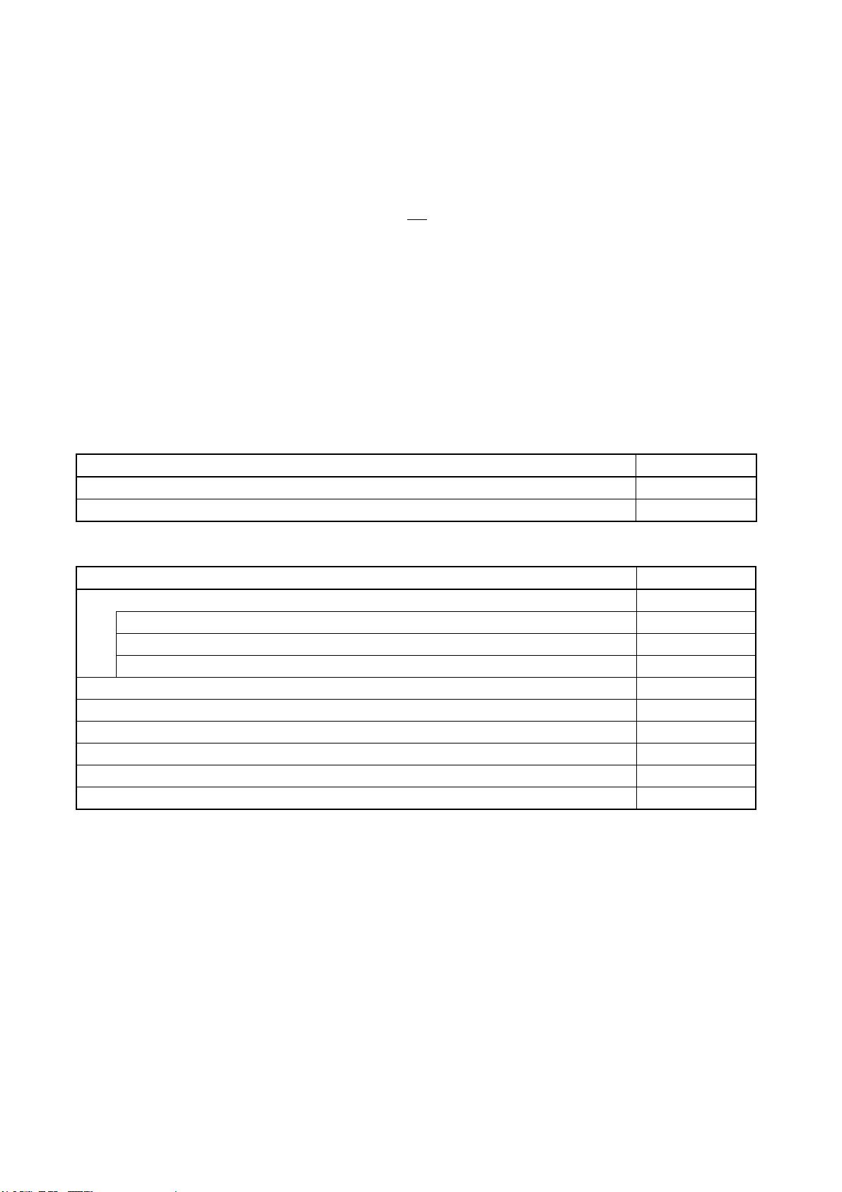
Organization The RL78/G13 manual is separated into two parts: this manual and the instructions edition
(common to the RL78 Microcontroller).
RL78/G13
User’s Manual
(This Manual)
RL78 Microcontroller
User’s Manual
Software
● Pin functions
● Internal block functions
● Interrupts
● Other on-chip peripheral functions
● Electrical specifications
● CPU functions
● Instruction set
● Explanation of each instruction
How to Read This Manual It is assumed that the readers of this manual have general knowledge of electrical
engineering, logic circuits, and microcontrollers.
● To gain a general understanding of functions:
→ Read this manual in the order of the CONTENTS. The mark “<R>” shows major
revised points. The revised points can be easily searched by copying an “<R>” in the
PDF file and specifying it in the “Find what:” field.
● How to interpret the register format:
→ For a bit number enclosed in angle brackets, the bit name is defined as a reserved
word in the assembler, and is defined as an sfr variable using the #pragma sfr
directive in the compiler.
● To know details of the RL78 Microcontroller instructions:
→ Refer to the separate document RL78 Family User's Manual: Software
(R01US0015E).
Conventions Data significance: Higher digits on the left and lower digits on the right
Active low representations: ××× (overscore over pin and signal name)
Note: Footnote for item marked with Note in the text
Caution: Information requiring particular attention
Remark: Supplementary information
Numerical representations: Binary
...
×××× or ××××B
Decimal
...
××××
Hexadecimal
...
××××H
Related Documents The related documents indicated in this publication may include preliminary versions.
However, preliminary versions are not marked as such.
Documents Related to Devices
Document Name Document No.
RL78/G13 User’s Manual Hardware This manual
RL78 Family User's Manual: Software R01US0015E
Documents Related to Flash Memory Programming
Document Name Document No.
PG-FP5 Flash Memory Programmer User’s Manual ―
RL78, 78K, V850, RX100, RX200, RX600 (Except RX64x), R8C, SH
R20UT2923E
Common
R20UT2922E
Setup Manual
R20UT0930E
PG-FP6 Flash Memory Programmer User's Manual R20UT4025E
E1, E20 Emulator User's Manual R20UT0398E
E2 Emulator User's Manual R20UT3538E
E2 Lite Emulator User's Manual R20UT3240E
Renesas Flash Programmer Flash Memory Programming Software User’s Manual R20UT4066E
Renesas Flash Development Toolkit User’s Manual R20UT0508E
Caution The related documents listed above are subject to change without notice. Be sure to use the latest
version of each document when designing.


