ADS1118 PDF
需积分: 10 189 浏览量
2014-07-28
10:40:33
上传
评论
收藏 671KB PDF 举报

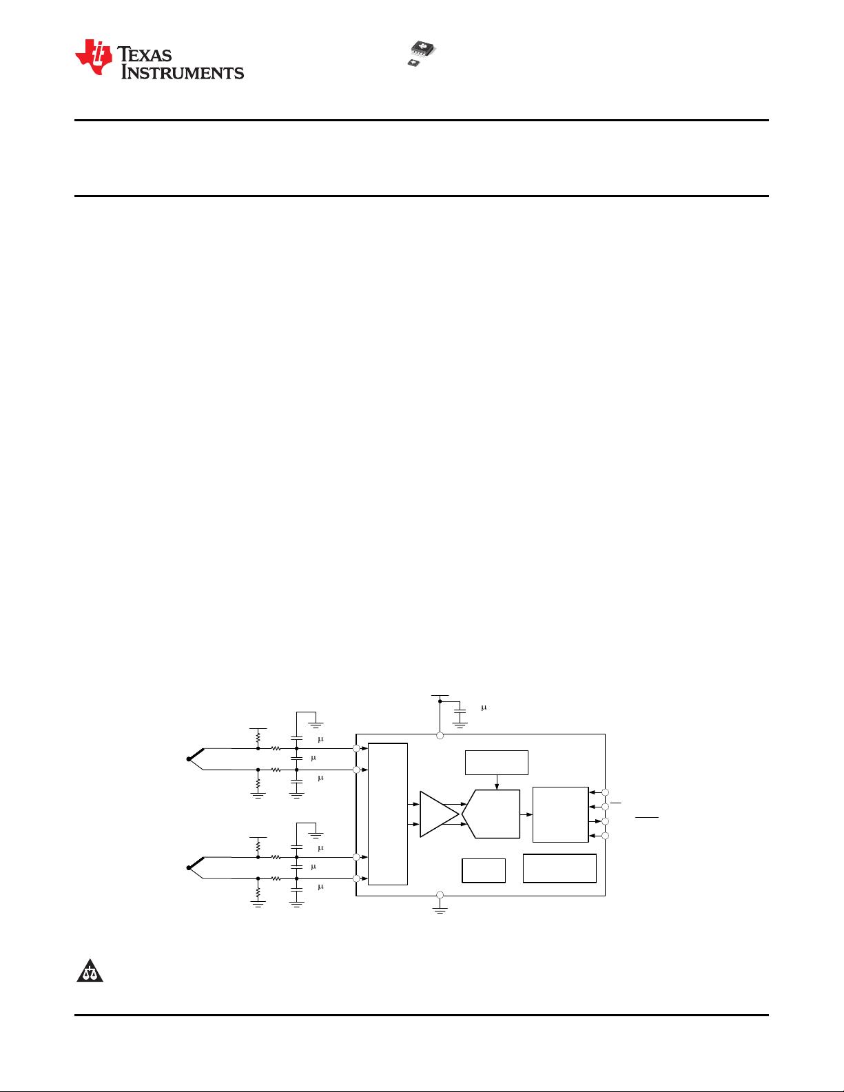
SPI
Interface
Oscillator
Voltage
Reference
High Accuracy
Temp Sensor
MUX
PGA
16-bit Ȉǻ
ADC
GND
2V
500ȍ
500ȍ
0.1 F
1 F
0.1 F
GND
1Mȍ
1Mȍ
GND
2V
500ȍ
500ȍ
1 F
0.1 F
GND
1Mȍ
GND
2V
0.1 F
0.1 F
GND
AIN0
AIN1
AIN2
AIN3
SCLK
CS
VDD
GND
DOUT/DRDY
DIN
ADS1118
1Mȍ
GND
GND
ADS1118
www.ti.com
SBAS457A –OCTOBER 2010–REVISED JULY 2011
Ultra-Small, Low-Power, SPI™-Compatible, 16-Bit
Analog-to-Digital Converter and Temperature Sensor with Internal Reference
Check for Samples: ADS1118
1
FEATURES
DESCRIPTION
The ADS1118 is a precision analog-to-digital
23
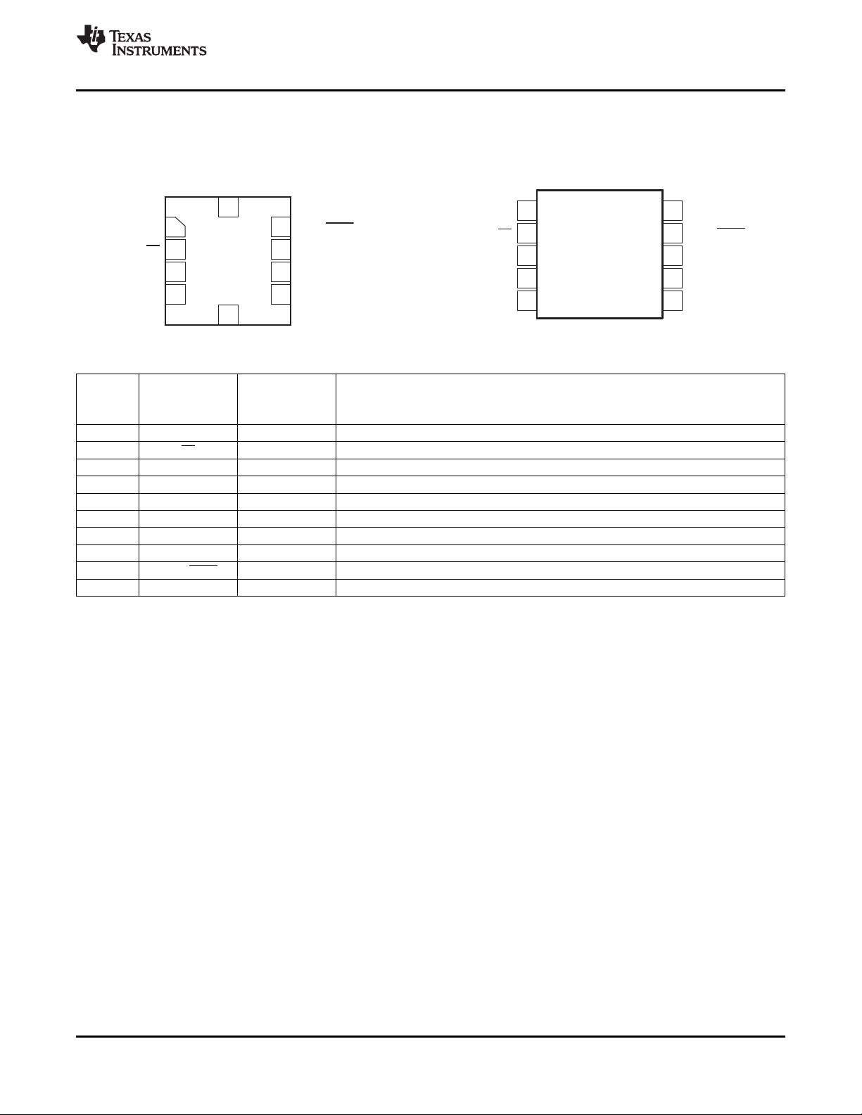
• Ultra-Small QFN Package:
converter (ADC) with 16 bits of resolution offered in
2mm × 1,5mm × 0,4mm
an ultra-small, leadless QFN-10 package or an
• Wide Supply Range: 2.0V to 5.5V
MSOP-10 package. The ADS1118 is designed with
• Low Current Consumption:
precision, power, and ease of implementation in
– Continuous Mode: Only 150μA
mind. The ADS1118 features an onboard reference
and oscillator. Data are transferred via a serial
– Single-Shot Mode: Auto Shutdown
peripheral interface (SPI). The ADS1118 operates
• Programmable Data Rate:
from a single power supply ranging from 2V to 5.5V.
8SPS to 860SPS
• Single-Cycle Settling
The ADS1118 can perform conversions at rates up to
860 samples per second (SPS). An onboard
• Internal Low-Drift Voltage Reference
programmable gain amplifier (PGA) is available on
• Internal Temperature Sensor:
the ADS1118 that offers input ranges from the supply
– 0.5°C Max Error
to as low as ±256mV. This range allows both large
• Internal Oscillator
and small signals to be measured with high
resolution. The ADS1118 also features an input
• Internal PGA
multiplexer (MUX) that provides two differential or
• Four Single-Ended or Two Differential Inputs
four single-ended inputs. The ADS1118 can also
function as a high-accuracy temperature sensor. This
APPLICATIONS
temperature sensor can be used for system-level
• Temperature Measurement:
temperature monitoring or cold junction compensation
for thermocouples.
– Thermocouple Measurement
– Cold Junction Compensation
The ADS1118 operates either in continuous
– Thermistor Measurement
conversion mode or a single-shot mode that
automatically powers down after a conversion.
• Portable Instrumentation
Single-shot mode significantly reduces current
• Factory Automation and Process Controls
consumption during idle periods. The ADS1118 is
specified from –40°C to +125°C.
1
Please be aware that an important notice concerning availability, standard warranty, and use in critical applications of Texas
Instruments semiconductor products and disclaimers thereto appears at the end of this data sheet.
2SPI is a trademark of Motorola.
3All other trademarks are the property of their respective owners.
PRODUCTION DATA information is current as of publication date.
Copyright © 2010–2011, Texas Instruments Incorporated
Products conform to specifications per the terms of the Texas
Instruments standard warranty. Production processing does not
necessarily include testing of all parameters.

剩余33页未读,继续阅读
资源评论


