txb0108 datasheet
需积分: 9 48 浏览量
2012-10-21
22:34:47
上传
评论
收藏 648KB PDF 举报

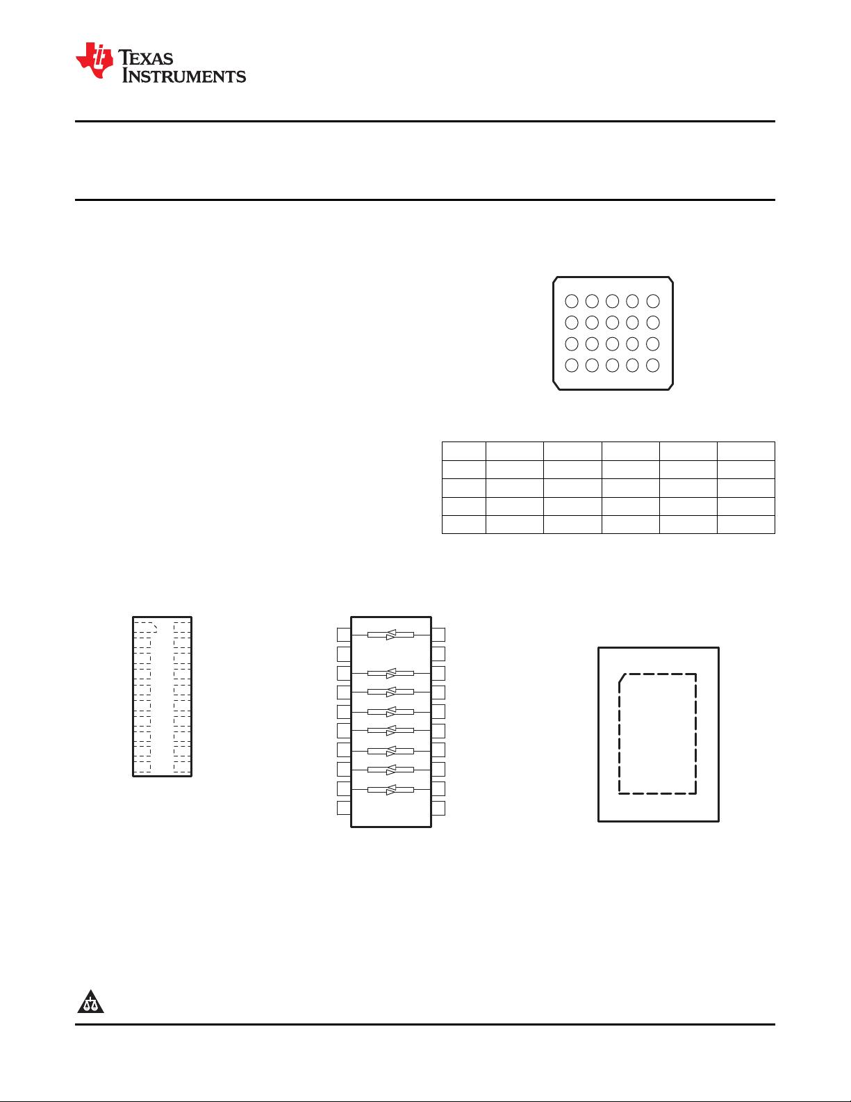
GXY OR ZXY PACKAGE
(BOTTOM VIEW)
A
B
C
D
21 3 4 5
20
19
16
15
14
13
1
2
5
6
7
8
PW PACKAGE
(TOP VIEW)
18
17
12
11
3
4
9
10
RGY PACKAGE
(TOP VIEW)
1 20
10 11
2
3
4
5
6
7
8
9
19
18
17
16
15
14
13
12
V
CCB
B2
B3
B4
B5
B6
B7
B8
V
CCA
A2
A3
A4
A5
A6
A7
A8
GND
B1
A1
OE
V
CCB
B2
B3
B4
B5
B6
B7
B8
GND
V
CCA
A1
A2
A3
A4
A5
A6
A7
A8
OE
B1
B1
B2
B3
B4
A2
A3
A4
1
2
3
4
20
19
18
17
V
CCB
GND
B5
B6
OE
A5
A6
5
6
7
8
16
15
14
13
B7
B8
A7
A8
9
10
12
11
A1
V
CCA
DQS PACKAGE
(TOP VIEW)
TXB0108
www.ti.com
SCES643B –NOVEMBER 2006–REVISED FEBRUARY 2010
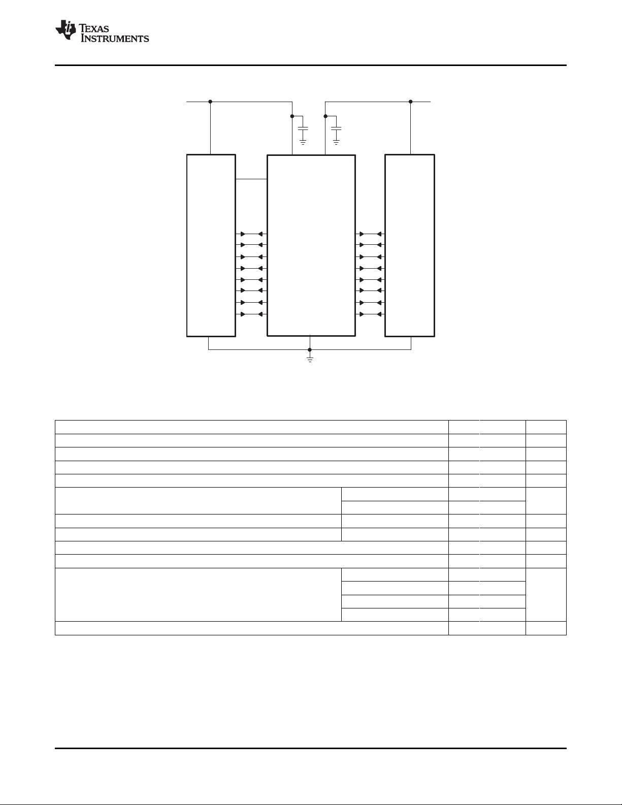
8-BIT BIDIRECTIONAL VOLTAGE-LEVEL TRANSLATOR
WITH AUTO-DIRECTION SENSING AND ±15-kV ESD PROTECTION
Check for Samples: TXB0108
1
FEATURES
• 1.2 V to 3.6 V on A Port and 1.65 to 5.5 V on
B Port (V
CCA
≤ V
CCB
)
• V
CC
Isolation Feature – If Either V
CC
Input Is at
GND, All Outputs Are in the High-Impedance
State
• OE Input Circuit Referenced to V
CCA
• Low Power Consumption, 4-mA Max I
CC
• I
off
Supports Partial-Power-Down Mode
Operation
• Latch-Up Performance Exceeds 100 mA Per
TERMINAL ASSIGNMENTS
JESD 78, Class II
(20-Ball GXY/ZXY Package)
• ESD Protection Exceeds JESD 22
1 2 3 4 5
– A Port
D V
CCB
B2 B4 B6 B8
– 2000-V Human-Body Model (A114-B)
C B1 B3 B5 B7 GND
– 1000-V Charged-Device Model (C101)
B A1 A3 A5 A7 OE
A V
CCA
A2 A4 A6 A8
– B Port
– ±15-kV Human-Body Model (A114-B)
– 1000-V Charged-Device Model (C101)
1
Please be aware that an important notice concerning availability, standard warranty, and use in critical applications of Texas
Instruments semiconductor products and disclaimers thereto appears at the end of this data sheet.
PRODUCTION DATA information is current as of publication date.
Copyright © 2006–2010, Texas Instruments Incorporated
Products conform to specifications per the terms of the Texas
Instruments standard warranty. Production processing does not
necessarily include testing of all parameters.


剩余21页未读,继续阅读
资源评论


