Biss转码芯片MB4资料Ic-Haus

preliminary preliminary
iC-MB4
BiSS INTERFACE MASTER
Rev A1, Page 1/40
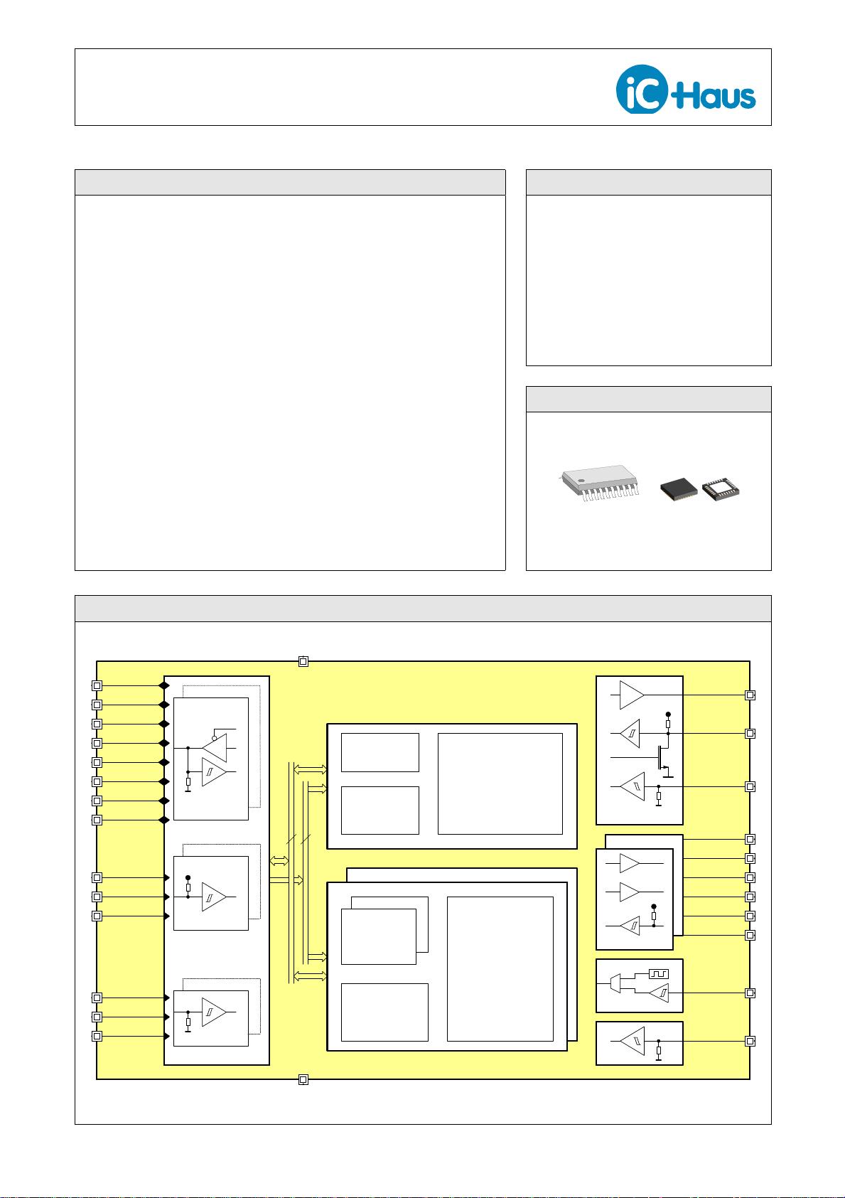
FEATURES
♦ Bidirectional BiSS communication with up to 8 slaves
♦ Supports SSI protocol for unidirectional data transmission
♦ Synchronous sensor data acquisition with cyclic transfer at
data rates of up to 10 Mbit/s
♦ Configurable interface with TTL, CMOS, RS422 or LVDS
♦ Slave register operations during cyclic data transfers
♦ Automatic compensation of line delays and conversion times
♦ Data lengths of up to 64 bit for sensor data,
configurable for each slave
♦ Data verification by CRC polynomials of up to 16 bits per slave
♦ Separate memory banks enable free controller access during
BiSS sensor data transfers
♦ 64 bytes memory for bidirectional slave register
communication
♦ Parallel interface with 8 bit data/address bus services Intel and
Motorola devices with combined data and address bus
♦ Serial controller communication by SPI
TM
-compatible mode
♦ Single 3 V to 5 V supply, industrial temperature range
APPLICATIONS
♦ Bidirectional communication in
multi sensor systems
♦ Linear and rotary encoders
♦ Motor feedback systems
♦ PLC systems
♦ Drives
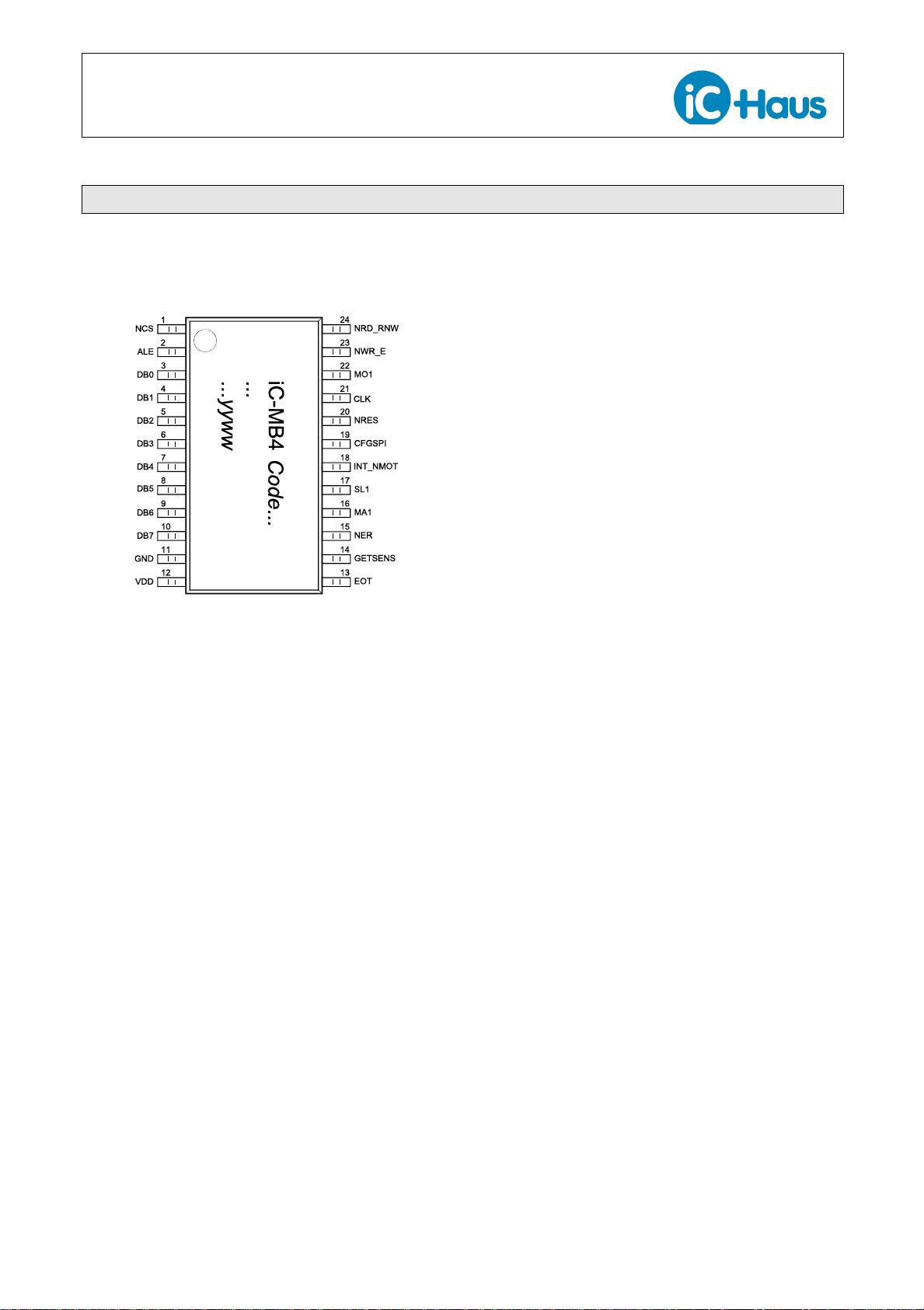
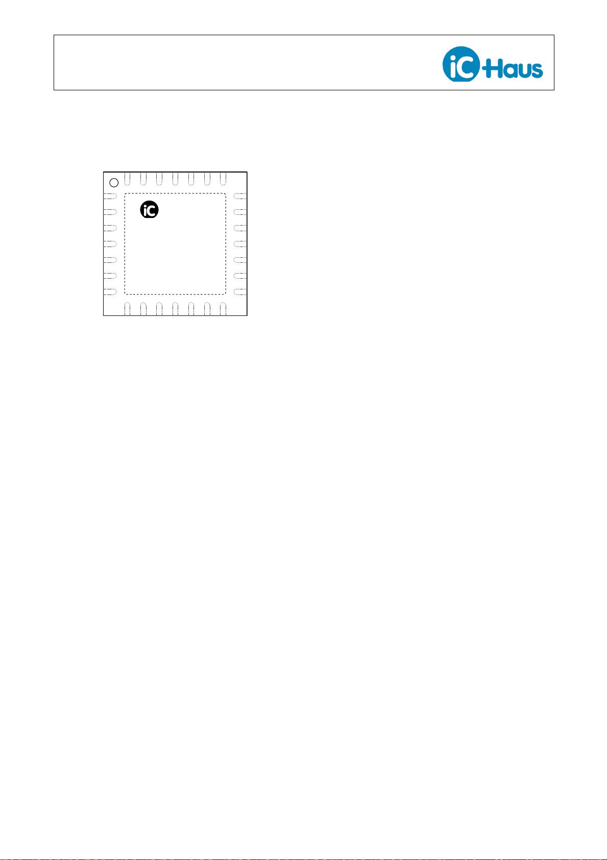
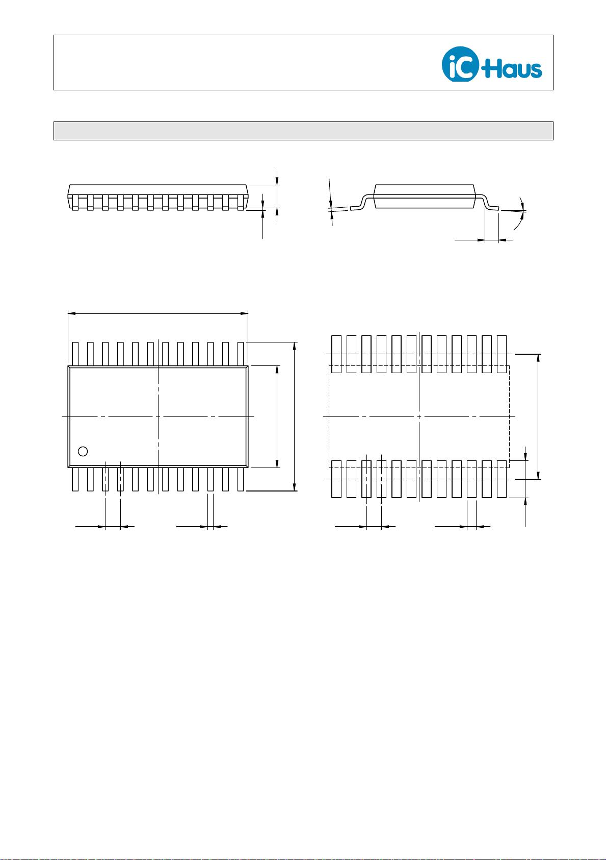
PACKAGES
TSSOP24 QFN28
BLOCK DIAGRAM
VDD
PROCESS DATA
OSCILLATOR
HOST INTERFACE RESET
CTRL PORTS
BANK 1
BiSS INTERFACE
VDD
VDD
INSTANCE 1
BANK 2
sample CDS
measure busy
FRAME CONTROLLER
send busy
request sensor data
send acknowledge
DATA BUS
ADDRESS BUS
8 8
CHANNEL 1
iC-MB4
analyse wire delay
INSTANCE 2
CHANNEL 2
16 BYTE RAM
PARAMETER
CONTROL
CONFIG
PROCESS
4 x 32 BIT RAM
DATA
DATA
PROCESS
4 x 64 BIT RAM
CONTROLLER
calculate actuator crc
send actuator data
receive sensor data
check sensor data
64 BYTE RAM
send start
calculate control frame
send CDM
GND
NCS
MO1
DB7
INT_NMOT
SL2_NSL1
MO2_NMO1
DB5
NRES
DB6
CLK
VDD
NWR_E
DB4
EOT
NER
GETSENS
DB2
DB1
DB0
NRD_RNW
CFGSPI
DB3
ALE
MA2_NMA1
MA1
SL1
Copyright © 2014 iC-Haus http://www.ichaus.com
剩余39页未读,继续阅读
资源评论

 boilingcity_12014-10-06ic-mb4 datasheet,很有用,感谢分享


