as3992-datasheet


AS3992
UHF RFID Single Chip Reader EPC Class1 Gen2 Compatible
www.austriamicrosystems.com/AS3992 Revision 1.0 1 - 52
Data Sheet
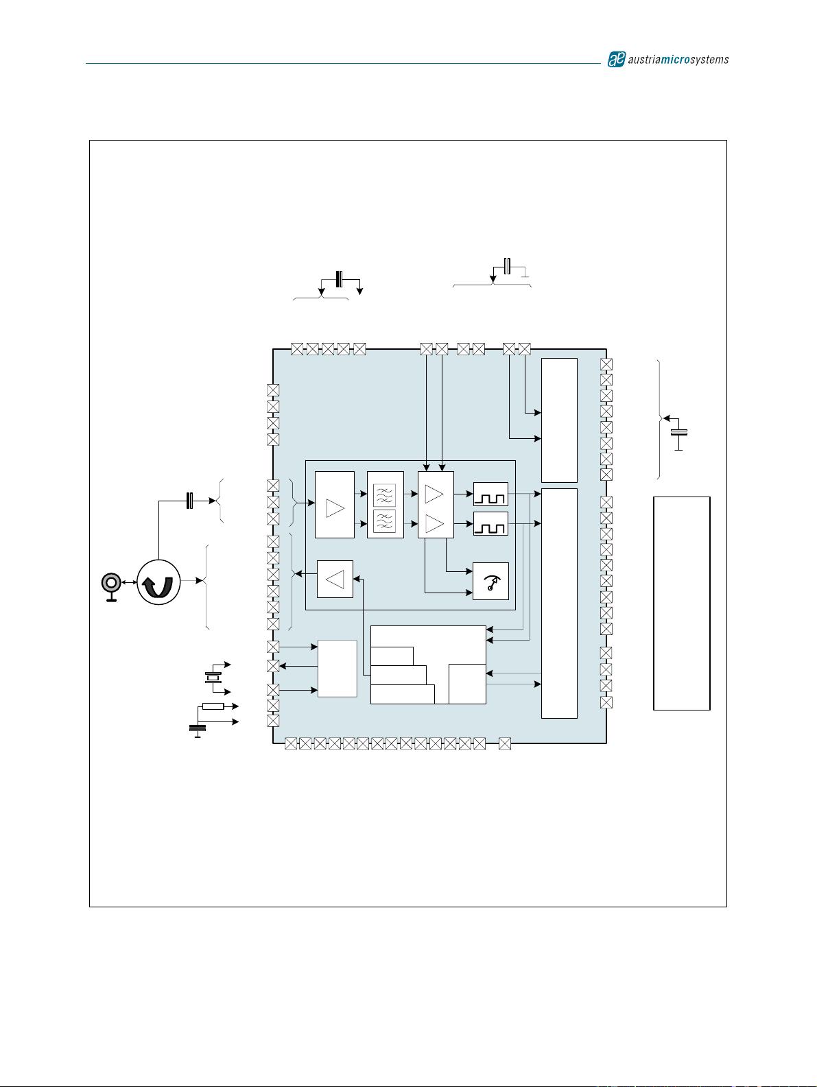
1 General Description
The AS3992 UHF Gen2 Reader chip is an integrated analog front-
end and provides protocol handling for ISO180006c/b 900MHz RFID
reader systems. Equipped with multiple built-in programming
options, the device is suitable for a wide range of UHF RFID
applications.
The AS3992 is pin to pin and firmware compatible with the previous
AS3990/91 IC's. It offers improved receive sensitivity to -86dB,
programmable Rx Dense Reader Mode (DRM) filters on chip and
pre-distortion. Fully scalable, the AS3992 is ideal for longer range
and higher power applications.
Offering DRM filtering on chip, combined with improved sensitivity
and pre-distortion allows the AS3992 to be the only true world wide
shippable IC. The reader configuration is achieved through setting
control registers allowing fine tuning of different reader parameters.
Parallel or serial interface can be selected for communication
between the host system (MCU) and the reader IC. When hardware
coders and decoders are used for transmission and reception, data
is transferred via 24 bytes FIFO register. In case of direct
transmission or reception, coders and decoders are bypassed and
the host system can service the analog front end in real time.
The transmitter generates 20dBm output power into 50Ω load and is
capable of ASK or PR-ASK modulation. The integrated supply
voltage regulators ensure supply rejection of the complete reader
system.
The transmission system comprises low level data coding. Automatic
generation of FrameSync, Preamble, and CRC is supported.
The receiver system allows AM and PM demodulation. The receiver
also comprises automatic gain control option (patent pending) and
selectable gain and signal bandwidth to cover a range of input link
frequency and bit rate options. The signal strength of AM and PM
modulation is measured and can be accessed in RSSI register. The
receiver output is selectable between digitized sub-carrier signal and
any of integrated sub-carrier decoders. Selected decoders deliver bit
stream and data clock as outputs.
The receiver system also comprises framing system. This system
performs the CRC check and organizes the data in bytes. Framed
data is accessible to the host system through a 24 byte FIFO
register.
To support external MCU and other circuitry a 3.3V regulated supply
and clock outputs are available. The regulated supply has 20mA
current capability.
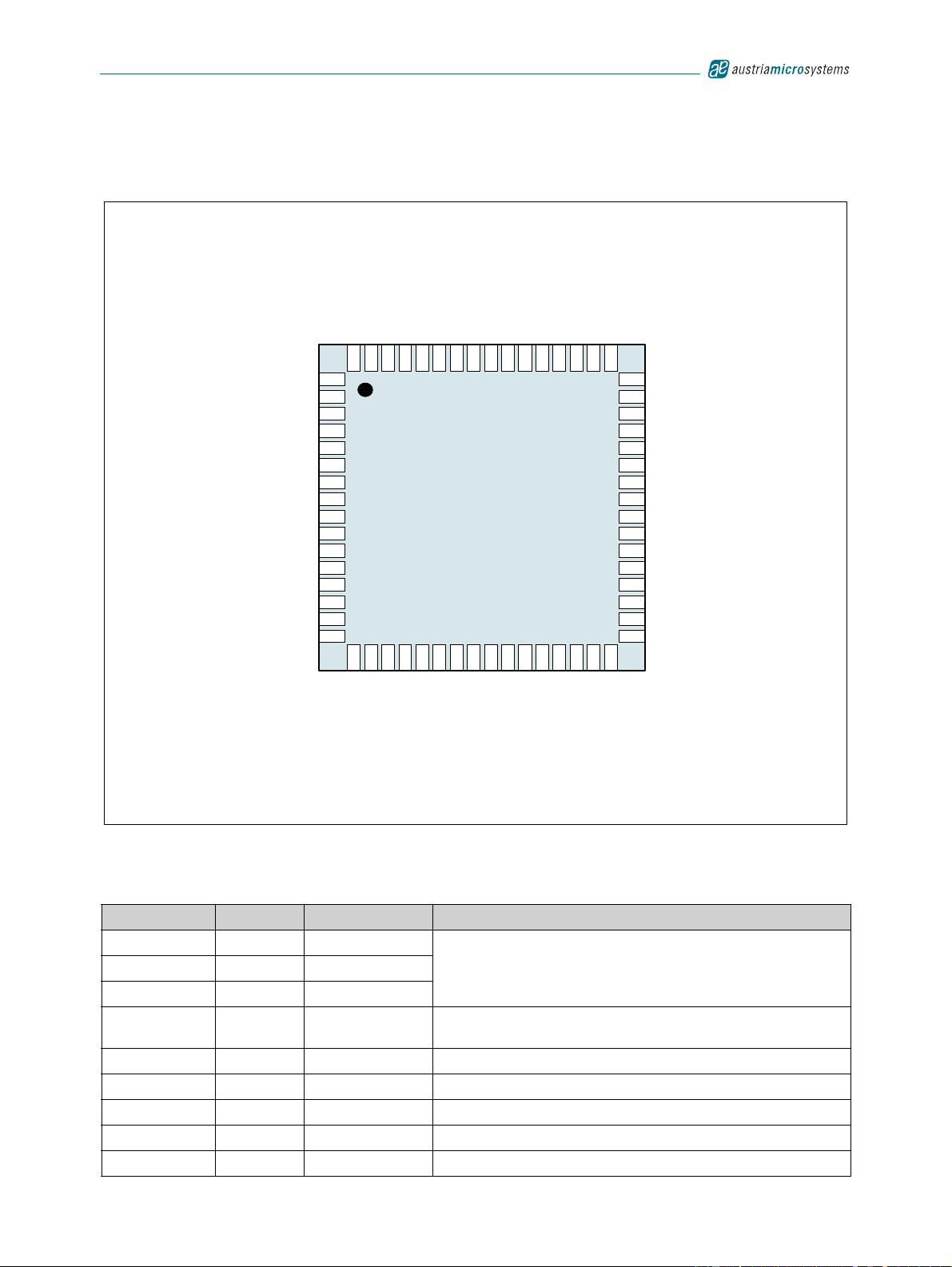
The AS3992 is available in a 64-pin QFN (9mm x 9mm), ensuring
the smallest possible footprint.
2 Key Features
ISO18000-6C (EPC Gen2) full protocol support
ISO18000-6A,B compatibility in direct mode
Programmable Dense Reader Mode filters on chip allowing a
true World Wide Shippable device.
Improved receive sensitivity to -86dBm
On chip pre-distortion meaning improved external PA efficiency
Integrated low level transmission coding, Integrated low level
decoders
Integrated data framing, Integrated CRC checking
Parallel 8-bit or serial 4-pin SPI interface to MCU using 24 bytes
FIFO
Voltage range for communication to MCU between 1.8V and
5.5V
Can be powered by USB with no need for step conversion from
4.1 to 5.5 Volt.
Selectable clock output for MCU
Integrated supply voltage regulator (20mA), which can be used
to supply MCU and other external circuitry
Integrated supply voltage regulator for the RF output stage,
providing rejection to supply noise
Internal power amplifier (20dBm) for short range applications
Modulator using ASK or PR-ASK modulation
Adjustable ASK modulation index
AM & PM demodulation ensuring no “communication holes”
with automatic I/Q selection
Selectable reception gain, Reception automatic gain control
AD converter for measuring TX power using external RF power
detector
DA converter for controlling external power amplifier
Frequency hopping support
On-board VCO and PLL covering complete RFID frequency
range 840MHz to 960MHz
Oscillator using 20MHz crystal
Power down, standby and active mode available
3 Applications
The device is an ideal solution for UHF RFID reader systems and
hand-held UHF RFID readers.


剩余51页未读,继续阅读
资源评论

 ZHIMATANG272013-05-21很好 对我的帮助很大 正好在学习这个项目
 wwrwrews2015-04-21资源很好用,值得一看非常!

sparkle_q
- 粉丝: 0
- 资源: 2


最新资源
- 基于matlab实现夜间车牌识别程序(1).rar
- 基于matlab实现图像处理,本程序使用背景差分法对来往车辆进行检测和跟踪.rar
- 基于matlab实现视频监控中车型识别代码,自己写的,希望和大家多多交流.rar
- sdk.config
- 基于matlab实现配电网三相潮流计算方法,对几种常用的配电网潮流计算方法进行了对比分析.rar
- 基于matlab实现配电网潮流 经典33节点 前推回代法潮流计算 回代电流 前推电压 带注释.rar
- 基于matlab实现模拟退火遗传算法的车辆调度问题研究,用MATLAB语言加以实现.rar
- 基于matlab实现蒙特卡洛的的移动传感器节点定位算法仿真代码.rar
- 华中数控系统818用户说明书
- 基于matlab实现卡尔曼滤波器完成多传感器数据融合 对多个机器人的不同传感器数据进行融合估计足球精确位置.rar
资源上传下载、课程学习等过程中有任何疑问或建议,欢迎提出宝贵意见哦~我们会及时处理!
点击此处反馈


