没有合适的资源?快使用搜索试试~ 我知道了~
LDO-ID9301 datasheet
需积分: 17 3 下载量 177 浏览量
2018-11-12
14:31:09
上传
评论 1
收藏 247KB PDF 举报
温馨提示
试读
15页
LDO-ID9301稳压降压芯片参考数据手册(含SC70-5,SOT23-3,SOT23-5,SOT89-3,:SOT89-3-L等封装)
资源推荐
资源详情
资源评论
iD9301
Low Noise 300mA LDO Regulator
Apr. 2011 1 Rev 0.8
General Description
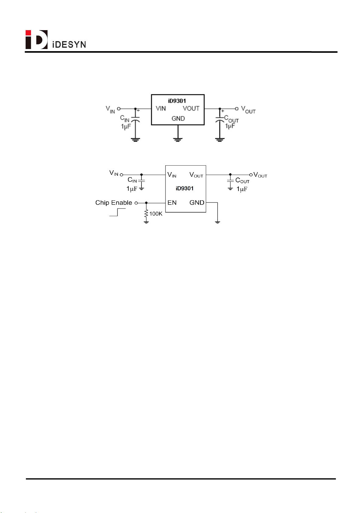
The iD9301 is a 300mA with fixed output voltage
options ranging from 1.5V, low dropout and low noise
linear regulator with high ripple rejection ratio and fast
turn-on time.
It includes a reference voltage source, an error
amplifier, driver transistors and an internal current
limiter. The current limiter’s holdback circuit operates
as a short protection.
The iD9301 works well with low ESR ceramic
capacitors, suitable for portable RF and wireless
battery-powered applications with stringent space
requirements and demanding performance. It also
offers ultra low noise output and has low quiescent
current.
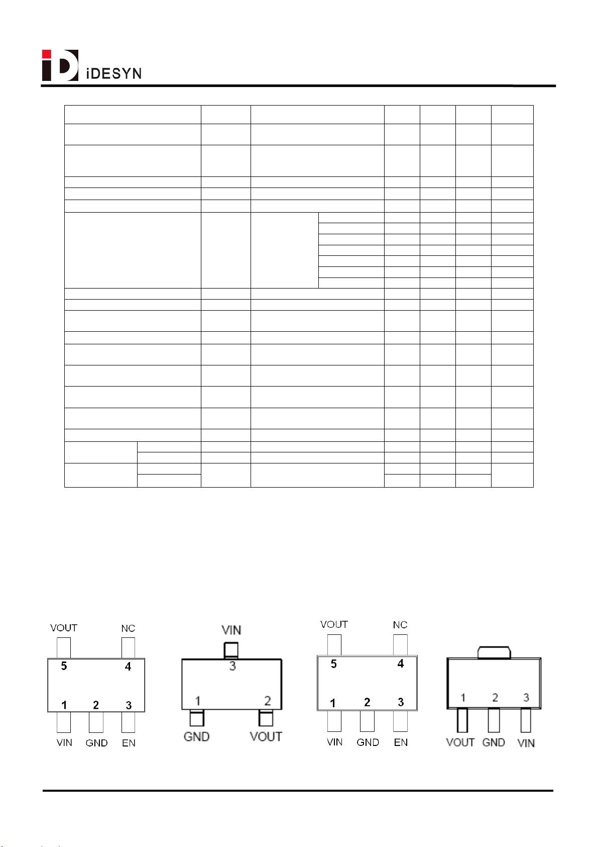
Ordering Information
iD9301 - □□ □□□ □
Package
C50:SC70-5
A30:SOT23-3
A50:SOT23-5
A20:SOT89-3
A21:SOT89-3-L Type
Output Voltage Voltage Code
1.5 15
1.8 18
2.5 25
2.7 27
2.8 28
3.0 30
3.3 33
Packing
R: Tape and Reel
Other voltage outputs may be available. For further
details, please contact an iDesyn sales or distributor.
Features
Low-Noise application
Wide 2.5V to 6V Operating Range
Quick Start-Up
Seven Fixed Voltage Options Available
Current Limiting Protection
Thermal Shutdown Protection
Low Dropout : 200mV @ 300mA
High Ripple Rejection 55dB@10Hz
Standby Current Less Than 0.1μ
A
Auto Discharge
Applications
Battery-Powered Equipment
Portable Instruments
Digital Camera
WLAN Communication
Hand-Held Instruments
Marking Information
Output Voltage
Type I:
Type II:
Type III:
1.5V
1.8V
2.5V
2.7V
2.8V
2.85V
F
H
L
S
O
U
:
:
:
:
:
:
3.0V
3.1V
3.2V
3.3V
3.5V
K
V
X
T
Y
:
:
:
:
:
SOT89-3
SOT23-3
SOT23-5
SC70-5
xxxxxx□x
9301
A1□xx
A1□x
Please use the table shown above for output voltage
indication on IC marking. For other marking
information, please contact our sales representative
directly or through an iDesyn distributor around your
location.
iD9301
Apr. 2011 2 Rev 0.8
Typical Application Circuit
Absolute Maximum Ratings
Recommended Operating Conditions
Supply Voltage V
IN
6V Input Voltage V
IN
2.5V to 6V
Power Dissipation, P
D
@ T
A
=25°C EN Input Voltage 0V to 5.5V
SC70-5 300mW Junction Temperature -40°C to 125°C
SOT23-3 & SOT23-5 400mW Ambient Operating Temperature -40°C to 85°C
SOT89-3 570mW
Thermal Resistance,
θ
ja
SC70-5 333°C/W
SOT23-3 & SOT23-5 250°C/W
SOT89-3 175°C/W
Lead Temperature 260 °C
Storage Temperature -65°C to 150°C
ESD Susceptibility
HBM (Human Body Mode) 4kV
MM (Machine Mode) 300V
iD9301
Apr. 2011 3 Rev 0.8
Electrical Characteristics (Unless otherwise specified V
IN
=5V, T
A
=25°C)
Parameters Symbo Condition Min Typ Max Units
Operating Voltage Range
(Note 2)
V
IN
2.5 6 V
V
IN
Discharge to Normal
Operation Power on Voltage
(Note 3)
0.4 V
Shutdown Supply Current I
SBY
V
EN
= GND, Shutdown 0.01 1 μA
Supply Current Limit I
Limit
R
LOAD
= 1Ω
360 400 mA
Quiescent Current I
Q
V
EN
≧ 1.2V,
I
OUT
= 0mA
90 130 μA
V
OUT
= 1.5V 1360 1800 mV
V
OUT
= 1.8V 1100 1500 mV
V
OUT
= 2.5V 580 800 mV
V
OUT
= 2.8V 410 500 mV
V
OUT
= 2.85V 390 490 mV
V
OUT
= 3V 300 400 mV
Dropout Voltage (Note 4) V
DROP
I
OUT
= 300mA
V
OUT
= 3.3V 200 300 mV
Standby Current I
STBY
V
EN
=GND 0.01 1 μA
EN Input Bias Current I
IBSD
V
EN
= GND or V
IN
0 100 nA
Line Regulation
ΔV
LINE
V
IN
= (V
OUT
+1V) to 5.5V,
I
OUT
= 1mA
6 mV/V
Load Regulation
ΔV
LOAD
1mA < I
OUT
< 300mA 40 mV
Output Noise Voltage eNO
10Hz to 100kHz
I
OUT
= 200mA, C
OUT
= 1μF
100 μV
RMS
Fast Discharge N-MOSFET
Turn On Resistance
R
DISCHARGE
V
IN
= 4V, V
EN
= 0V 35 Ω
Thermal Shutdown
Temperature
T
SD
165
°C
Thermal Shutdown
Temperature Hysteresis
ΔT
SD
30
°C
Output Voltage Accuracy
ΔV
OUT
I
OUT
= 1mA -2 +2 %
Logic-Low V V
IL
V
IN
= 3V to 5.5V,Shutdown 0.4 V
EN Threshold
Logic-High V V
IH
V
IN
= 3V to 5.5V,Start-Up 1.2 V
f = 10Hz -55 Power Supply
Rejection Rate
PSRR C
OUT
= 1μF, I
OUT
= 10mA
dB
Note 1: Stresses listed as the above "Absolute Maximum Ratings" may cause permanent damage to the device. These
are for stress ratings. Functional operation of the device at these or any other conditions beyond those indicated in
the operational sections of the specifications is not implied. Exposure to absolute maximum rating conditions for
extended periods may remain possibility to affect device reliability.
Note 2:
V
IN (MIN)
=V
OUT
+V
DROPOUT
Note 3: When input voltage power off, the input capacitor voltage must be discharged under 0.4V. It will assure internal
circuitry properly work on next time.
Note 4: The dropout voltage is defined as (V
IN
-V
OUT
) when V
OUT
is 100mV below the target value of V
OUT
.
Pin Configurations (Top View)
SC70-5 SOT23-3 SOT23-5 SOT89-3
剩余14页未读,继续阅读
资源评论
_Tic_
- 粉丝: 5
- 资源: 11
上传资源 快速赚钱
- 我的内容管理 展开
- 我的资源 快来上传第一个资源
- 我的收益 登录查看自己的收益
- 我的积分 登录查看自己的积分
- 我的C币 登录后查看C币余额
- 我的收藏
- 我的下载
- 下载帮助
安全验证
文档复制为VIP权益,开通VIP直接复制
信息提交成功