没有合适的资源?快使用搜索试试~ 我知道了~
OM8443-20 datasheet,最新芯片
需积分: 14 4 下载量 132 浏览量
2022-10-29
22:54:11
上传
评论
收藏 1.65MB PDF 举报
温馨提示
试读
26页
原来的汉天下,现在的昂瑞威芯片,Multimode Multiband (MMMB) Power Amplifier (PA) ,适合5G手机
资源详情
资源评论
资源推荐
www.onmicro.com.cn 1 of 26
Beijing OnMicro Electronics Confidential Information.
Products and Product Information are Subject to Change Without Notice.
Applications
Multiband 3G / LTE handsets
WCDMA Bands
I, II, III, IV, V, VIII, IX
TD-SCDMA Bands
34, 39
FDD LTE Bands
1, 2, 3, 4, 5, 7, 8, 9, 12,
13, 17, 20, 25, 26, 28,
30, 71
TDD LTE Bands
34, 38, 39, 40, 41
CDMA2000 Bands
BC0, BC1, BC4, BC6,
BC010, BC015
Product Features
- Two T/R (RX) ports and 14 outputs
- Dual Low Band RF inputs support separate transceiver
outputs or interstage filtering
- Industry-leading PAE for 3G/4G
- Optimized for APT DCDC operation
- Fully programmable Mobile Industry Processor Interface
(MIPI) control
- MIPI programmable bias modes optimize best efficiency /
linearity trade-off for 3G and 4G; minimizes DG09 for 3G.
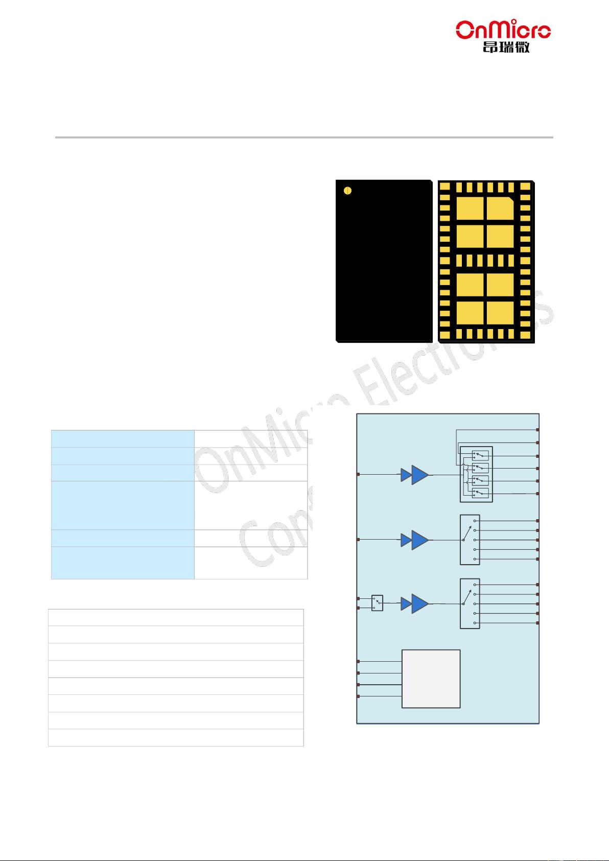
- Small package: 4.0 mm × 6.8 mm × 0.83 mm, LGA 42 pad
configuration
-Ultra low harmonics leakage from LB TX ports to MB TX
ports, suitable for downlink carrier aggregation
3G/4G Modulation Scheme
WCDMA Voice Release 99
HSDPA categories
HSUPA
HSPA+
TD-SCDMA
LTE 1.4, 3, 5, 10, 15, 20 MHz Channel BW
TDD-LTE
CDMA2000
OM8443-20
RFIN_L2
RFIN_L1
VBATT
VIO
SCLK
SDATA
RFIN_M
RFIN_H
MB1
MB3
MB4
MB5
HB1
HB2
HB3
T/R1
T/R2
MB2
HB4
LB4
LB2
LB1
LB5
LB3
MIPI_RFFE
CMOS
Controller
Figure 1 Functional Block Diagram.
Datasheet
Multimode Multiband (MMMB) Power Amplifier (PA)
Module
22
29
36
8
2
3
4
5
6
7
9
10
11
30
31
27
32
28
33
35
34
26
25
24
23
42
37
38
39
40
41
16
21
20
19
18
17
OM8443-20
OM8443-20 DataSheet
www.onmicro.com.cn 2 of 26
Beijing OnMicro Electronics Confidential Information.
Products and Product Information are Subject to Change Without Notice.
Absolute Maximum Conditions
Parameters
Symbol
Minimum
Maximum
Units
Supply Voltage (RF off)
VBATT, VCC
6.0
V
Supply Voltage (RF on)
VBATT, VCC
5.0
V
Input RF Power
PIN
+10
dBm
Digital Control Lines
VIO,SCLK,SDATA
3
V
Operating Temperature
T
CASE
-45
+100
o
C
Storage Temperature
T
STG
-55
+150
o
C
ESD Human Body Mode
ANSI/JEDEC/EDSA
standard JS-001-2010
Analog/Digital
I/O
ESD_HBM
-2000
2000
V
RF Pins
ESD_HBM
-1500
1500
V
VBATT/VCC
ESD_HBM
-6000
6000
V
Note:
1. Exposure to maximum rating conditions for extended periods may reduce device reliability. There is no damage to
device with only one parameter set at the limit and all other parameters set at or below their typical value.
2. Case Operating Temperature (T
CASE
) refers to the temperature of the GROUND PAD at the underside of the package.
Recommended Operating Conditions
Note: T
A
range= T
RANGE
for ETC, assuming T
CASE
- T
A
=15
o
C with PA self-heating in the thermal environments of EVB. For
poor heat dissipation applications, T
CASE
should be checked to avoid exceeding the maximum T
CASE
range.
Parameters
Symbol
Min.
Typ.
Max.
Units
VBATT
VBATT
3.1
3.4
4.6
V
VCC1,VCC2,VCC2_2
VCC
0.55
3.4
4.6
V
Leakage Current (VBATT=3.4V)
I
BATT_LK
10
µA
Leakage Current
(VCC1,VCC2,VCC2_2=3.4V)
I
CC_LK
10
µA
MIPI Supply(VIO)
VIO
1.65
1.8
1.95
V
Low MIPI Signal Level
V
MIPI_LOW
0
0.2*VIO
V
High MIPI Signal Level
V
MIPI_HIGH
0.8*VIO
1.0*VIO
V
Operating Temperature
T
A
-40
+25
+85
o
C
Product Description
OM8443-20 is a hybrid multimode multiband (MMMB) Power Amplifier Module (PAM) that supports 3G/4G handsets
and operates efficiently in CDMA, WCDMA, TD-SCDMA, and LTE modes. The module is fully programmable through a
Mobile Industry Processor Interface (MIPI).
The PAM consists of a 3G/4G PA blocks for low, high, and mid-bands, and a Multi-Function Control (MFC) block, RF
input/output ports internally matched to 50 ohm to reduce the number of external components. A CMOS integrated
circuit uses standard MIPI controls to provide the internal MFC interface and operation. Extremely low leakage current
maximizes handset standby time. The devices packaged in a small LGA package. (4.0 mm x 6.8 mm x 0.83 mm)
OM8443-20 DataSheet
www.onmicro.com.cn 3 of 26
Beijing OnMicro Electronics Confidential Information.
Products and Product Information are Subject to Change Without Notice.
MIPI RFFE Standard Register Map (1 of 2)
Register 0, Address: 0x00 (PA_CTRL0)
Register 0
Description
Default
Notes
[7]
Trigger Select
0
0 = Trigger 0, 1, 2 or’ d together
1 = Trigger 0, 1, 2 fire independently
[6:3]
PA Band Select Control
Mode
0000
Control Mode
0000 = PA's Disabled
0001 = LB1_TX
0010 = LB2_TX
0011 = LB3_TX
0100 = LB4_TX
0101 = LB5_TX
0110 = MB1_TX
0111 = MB2_TX
1000 = MB3_TX
1001 = MB4_TX
1010 = MB5_TX
1011 = HB1_TX
1100 = HB2_TX
1101 = HB3_TX
1110 = HB4_TX
1111 = PA's Disabled (High Switch isolation)
[2]
PA Enable
0
PA Enable
0 = PA Off
1 = PA On
[1]
Reserved
0
[0]
LB Input Switch
0
LB Input
0 = RFIN_L1 (default for MB/HB operation)
1 = RFIN_L2
Register 1, Address: 0x01 (BIAS_CTRL1)
Register 1
Description
Default
Notes
[7:4]
PA Bias1
0000
Range 0000-1111
Set PA Icq1
[3:0]
PA Bias2
0000
Range 0000-1111
Set PA Icq2
OM8443-20 DataSheet
www.onmicro.com.cn 4 of 26
Beijing OnMicro Electronics Confidential Information.
Products and Product Information are Subject to Change Without Notice.
MIPI RFFE Standard Register Map (2 of 2)
Register 2, Address: 0x02 (SWITCH_CTRL)
Register 2
Description
Default
Notes
[7:4]
Spare
0000
Spare
[3:0]
HB Switch RX Control
0000
Control Mode
0000 = Switch Off (Standby)
0001 = HB1 T/R2
0010 = HB2 T/R2
0011 = HB3 T/R1
0100 = HB4 T/R2
Others States = High Isolation
Register 28, Address: 0x1C (PM_TRIG)
Register 28
Description
Default
Notes
[7:6]
PWR_MODE
00
00 = Normal Operation (ACTIVE)
01 = Default Settings (STARTUP)
10 = Low Power (LOW POWER)
11 = Reserved
[5]
Trigger Mask 2
0
Trigger Enable: 0 Trigger Disable: 1
[4]
Trigger Mask 1
0
Trigger Enable: 0 Trigger Disable: 1
[3]
Trigger Mask 0
0
Trigger Enable: 0 Trigger Disable: 1
[2]
Trigger Register 2
0
Not supported
[1]
Trigger Register 1
0
1 = Latch Register 2 contents
[0]
Trigger Register 0
0
1 = Latch Register 0, 1, 3 contents
Register 29, Address: 0x1D (PROD_ID)
Register 29
Description
Default
Notes
[7:0]
Product ID
00101101
Product ID [7:0] = 0x2D
Register 30, Address: 0x1E (MAN_ID)
Register 30
Description
Default
Notes
[7:0]
Manufacturer ID
00111101
Manufacturer ID [7:0] = 0x3D
Register 31, Address: 0x1F (USID)
Register 31
Description
Default
Notes
[7:6]
Spare
00
[5:4]
Manufacturer ID
11
Manufacturer ID[9:8]
[3:0]
USID
1111
User ID = 0xF
剩余25页未读,继续阅读
shijuntao1985
- 粉丝: 1
- 资源: 72
上传资源 快速赚钱
- 我的内容管理 展开
- 我的资源 快来上传第一个资源
- 我的收益 登录查看自己的收益
- 我的积分 登录查看自己的积分
- 我的C币 登录后查看C币余额
- 我的收藏
- 我的下载
- 下载帮助
安全验证
文档复制为VIP权益,开通VIP直接复制
信息提交成功
评论0