没有合适的资源?快使用搜索试试~ 我知道了~
资源详情
资源评论
资源推荐
LatticeECP2/M Family Data Sheet
DS1006 Version 03.8, April 2011
www.latticesemi.com 1-1 DS1006 Introduction_01.8
July 2010 Data Sheet DS1006
© 2010 Lattice Semiconductor Corp. All Lattice trademarks, registered trademarks, patents, and disclaimers are as listed at www.latticesemi.com/legal. All other brand
or product names are trademarks or registered trademarks of their respective holders. The specifications and information herein are subject to change without notice.
Features
High Logic Density for System Integration
• 6K to 95K LUTs
• 90 to 583 I/Os
Embedded SERDES (LatticeECP2M Only)
• Data Rates 250 Mbps to 3.125 Gbps
• Up to 16 channels per device
PCI Express, Ethernet (1GbE, SGMII), OBSAI,
CPRI and Serial RapidIO.
sysDSP™ Block
• 3 to 42 blocks for high performance multiply and
accumulate
• Each block supports
– One 36x36, four 18x18 or eight 9x9 multipliers
Flexible Memory Resources
• 55Kbits to 5308Kbits sysMEM™ Embedded
Block RAM (EBR)
– 18Kbit block
– Single, pseudo dual and true dual port
– Byte Enable Mode support
• 12K to 202Kbits distributed RAM
– Single port and pseudo dual port
sysCLOCK Analog PLLs and DLLs
• Two GPLLs and up to six SPLLs per device
– Clock multiply, divide, phase & delay adjust
– Dynamic PLL adjustment
• Two general purpose DLLs per device
Pre-Engineered Source Synchronous I/O
• DDR registers in I/O cells
• Dedicated gearing logic
• Source synchronous standards support
– SPI4.2, SFI4 (DDR Mode), XGMII
– High Speed ADC/DAC devices
• Dedicated DDR and DDR2 memory support
– DDR1: 400 (200MHz) / DDR2: 533 (266MHz)
• Dedicated DQS support
Programmable sysI/O™ Buffer Supports
Wide Range Of Interfaces
• LVTTL and LVCMOS 33/25/18/15/12
• SSTL 3/2/18 I, II
• HSTL15 I and HSTL18 I, II
• PCI and Differential HSTL, SSTL
• LVDS, RSDS, Bus-LVDS, MLVDS, LVPECL
Flexible Device Configuration
• 1149.1 Boundary Scan compliant
• Dedicated bank for configuration I/Os
• SPI boot flash interface
• Dual boot images supported
• TransFR™ I/O for simple field updates
• Soft Error Detect macro embedded
Optional Bitstream Encryption
(LatticeECP2/M “S” Versions Only)
System Level Support
• ispTRACY™ internal logic analyzer capability
• On-chip oscillator for initialization & general use
•1.2V power supply
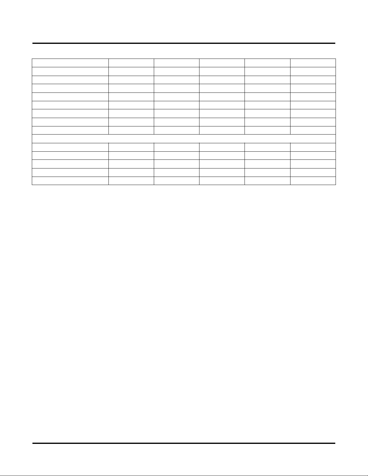
Table 1-1. LatticeECP2 (Including “S-Series”) Family Selection
Device ECP2-6 ECP2-12 ECP2-20 ECP2-35 ECP2-50 ECP2-70
LUTs (K) 6 12 21 32 48 68
Distributed RAM (Kbits) 1224426496136
EBR SRAM (Kbits) 55 221 276 332 387 1032
EBR SRAM Blocks 3 12 15 18 21 60
sysDSP Blocks 3 6 7 8 18 22
18x18 Multipliers 122428327288
GPLL + SPLL + DLL 2+0+2 2+0+2 2+0+2 2+0+2 2+2+2 2+4+2
Maximum Available I/O 190 297 402 450 500 583
Packages and I/O Combinations
144-pin TQFP (20 x 20 mm) 90 93
208-pin PQFP (28 x 28 mm) 131 131
256-ball fpBGA (17 x 17 mm) 190 193 193
484-ball fpBGA (23 x 23 mm) 297 331 331 339
672-ball fpBGA (27 x 27 mm) 402 450 500 500
900-ball fpBGA (31 x 31 mm) 583
LatticeECP2/M Family Data Sheet
Introduction
1-2
Introduction
Lattice Semiconductor LatticeECP2/M Family Data Sheet
Table 1-2. LatticeECP2M (Including “S-Series”) Family Selection
Introduction
The LatticeECP2/M family of FPGA devices is optimized to deliver high performance features such as advanced
DSP blocks, high speed SERDES (LatticeECP2M family only) and high speed source synchronous interfaces in an
economical FPGA fabric. This combination was achieved through advances in device architecture and the use of
90nm technology.
The LatticeECP2/M FPGA fabric is optimized with high performance and low cost in mind. The LatticeECP2/M
devices include LUT-based logic, distributed and embedded memory, Phase Locked Loops (PLLs), Delay Locked
Loops (DLLs), pre-engineered source synchronous I/O support, enhanced sysDSP blocks and advanced configu-
ration support, including encryption (“S” versions only) and dual boot capabilities.
The LatticeECP2M device family features high speed SERDES with PCS. These high jitter tolerance and low trans-
mission jitter SERDES with PCS blocks can be configured to support an array of popular data protocols including
PCI Express, Ethernet (1GbE and SGMII), OBSAI and CPRI. Transmit Pre-emphasis and Receive Equalization
settings make SERDES suitable for chip to chip and small form factor backplane applications.
The Lattice Diamond™ and ispLEVER
®
design software from Lattice allow large complex designs to be efficiently
implemented using the LatticeECP2/M FPGA family. Synthesis library support for LatticeECP2/M is available for
popular logic synthesis tools. The Diamond and ispLEVER tools use the synthesis tool output along with the con-
straints from its floor planning tools to place and route the design in the LatticeECP2/M device. The Diamond and
ispLEVER tools extract the timing from the routing and back-annotates it into the design for timing verification.
Lattice provides many pre-engineered IP (Intellectual Property) modules for the LatticeECP2/M family. By using
these IP cores as standardized blocks, designers are free to concentrate on the unique aspects of their design,
increasing their productivity.
Device ECP2M20 ECP2M35 ECP2M50 ECP2M70 ECP2M100
LUTs (K) 1934486795
sysMEM Blocks (18kb) 66 114 225 246 288
Embedded Memory (Kbits) 1217 2101 4147 4534 5308
Distributed Memory (Kbits) 41 71 101 145 202
sysDSP Blocks 6 8 22 24 42
18x18 Multipliers 24 32 88 96 168
GPLL+SPLL+DLL 2+6+2 2+6+2 2+6+2 2+6+2 2+6+2
Maximum Available I/O 304 410 410 436 520
Packages and SERDES / I/O Combinations
256-ball fpBGA (17 x 17 mm) 4 / 140 4 / 140
484-ball fpBGA (23 x 23 mm) 4 / 304 4 / 303 4 / 270
672-ball fpBGA (27 x 27 mm) 4 / 410 8 / 372
900-ball fpBGA (31 x 31 mm) 8 / 410 16 / 416 16 / 416
1152-ball fpBGA (35 x 35 mm) 16 / 436 16 / 520
www.latticesemi.com 2-1 DS1006 Architecture_02.0
July 2010 Data Sheet DS1006
© 2010 Lattice Semiconductor Corp. All Lattice trademarks, registered trademarks, patents, and disclaimers are as listed at www.latticesemi.com/legal. All other brand
or product names are trademarks or registered trademarks of their respective holders. The specifications and information herein are subject to change without notice.
Architecture Overview
Each LatticeECP2/M device contains an array of logic blocks surrounded by Programmable I/O Cells (PIC). Inter-
spersed between the rows of logic blocks are rows of sysMEM™ Embedded Block RAM (EBR) and rows of sys-
DSP™ Digital Signal Processing blocks, as shown in Figure 2-1. In addition, the LatticeECP2M family contains
SERDES Quads in one or more of the corners. Figure 2-2 shows the block diagram of ECP2M20 with one quad.
There are two kinds of logic blocks, the Programmable Functional Unit (PFU) and Programmable Functional Unit
without RAM (PFF). The PFU contains the building blocks for logic, arithmetic, RAM and ROM functions. The PFF
block contains building blocks for logic, arithmetic and ROM functions. Both PFU and PFF blocks are optimized for
flexibility, allowing complex designs to be implemented quickly and efficiently. Logic Blocks are arranged in a two-
dimensional array. Only one type of block is used per row.
The LatticeECP2/M devices contain one or more rows of sysMEM EBR blocks. sysMEM EBRs are large dedicated
18K fast memory blocks. Each sysMEM block can be configured in a variety of depths and widths of RAM or ROM.
In addition, LatticeECP2/M devices contain up to two rows of DSP Blocks. Each DSP block has multipliers and
adder/accumulators, which are the building blocks for complex signal processing capabilities.
The LatticeECP2M devices feature up to 16 embedded 3.125Gbps SERDES (Serializer / Deserializer) channels.
Each SERDES channel contains independent 8b/10b encoding / decoding, polarity adjust and elastic buffer logic.
Each group of four SERDES channels along with its Physical Coding Sub-layer (PCS) block, creates a quad. The
functionality of the SERDES/PCS Quads can be controlled by memory cells set during device configuration or by
registers that are addressable during device operation. The registers in every quad can be programmed by a soft
IP interface, referred to as the SERDES Client Interface (SCI). These quads (up to four) are located at the corners
of the devices.
Each PIC block encompasses two PIOs (PIO pairs) with their respective sysI/O buffers. The sysI/O buffers of the
LatticeECP2/M devices are arranged in eight banks, allowing the implementation of a wide variety of I/O standards.
In addition, a separate I/O bank is provided for the programming interfaces. PIO pairs on the left and right edges of
the device can be configured as LVDS transmit/receive pairs. The PIC logic also includes pre-engineered support
to aid in the implementation of high speed source synchronous standards such as SPI4.2, along with memory
interfaces including DDR2.
Other blocks provided include PLLs, DLLs and configuration functions. The LatticeECP2/M architecture provides
two General PLLs (GPLL) and up to six Standard PLLs (SPLL) per device. In addition, each LatticeECP2/M family
member provides two DLLs per device. The GPLLs and DLLs blocks are located in pairs at the end of the bottom-
most EBR row; the DLL block is located towards the edge of the device. The SPLL blocks are located at the end of
the other EBR/DSP rows.
The configuration block that supports features such as configuration bit-stream decryption, transparent updates
and dual boot support is located toward the center of this EBR row. The Ball Grid Array (BGA) package devices in
the LatticeECP2/M family supports a sysCONFIG™ port located in the corner between banks four and five, which
allows for serial or parallel device configuration.
In addition, every device in the family has a JTAG port. This family also provides an on-chip oscillator and soft error
detect capability. The LatticeECP2/M devices use 1.2V as their core voltage.
LatticeECP2/M Family Data Sheet
Architecture
2-2
Architecture
Lattice Semiconductor LatticeECP2/M Family Data Sheet
Figure 2-1. Simplified Block Diagram, ECP2-6 Device (Top Level)
Figure 2-2. Simplified Block Diagram, ECP2M20 Device (Top Level)
Programmable
Function Units
(PFUs)
Flexible sysIO Buffers:
LVCMOS, HSTL, SSTL,
LVDS, and other standards
sysDSP Blocks
Multiply and
Accumulate Support
sysMEM Block RAM
18kbit Dual Port
sysCLOCK PLLs and DLLs
Frequency Synthesis and
Clock Alignment
Flexible routing optimized
for speed, cost and routability
Configuration logic, including
dual boot and encryption.
On-chip oscillator and
soft-error detection.
Configuration port
Pre-engineered source
synchronous support
• DDR1/2
• SPI4.2
• ADC/DAC devices
Flexible sysIO
Buffers:
LVCMOS, HSTL
SSTL, LVDS
Pre-Engineered
Source Synchronous
Support
• DDR1/2
• SPI4.2
• ADC/DAC devices
SERDES
DSP Blocks
Multiply & Accumulate
Support
On-Chip
Oscillator
Programmable
Function Units
(PFUs)
Channel
3
Channel
2
Channel
1
Channel
0
sysMEM Block
RAM 18kbit Dual Port
Configuration
Logic, Including
dual boot and encryption,
and soft-error detection
Flexible Routing
optimized for speed,
cost & routability
sysCLOCK GPLLs
& GDLLs
Frequency Synthesis
& Clock Alignment
Configuration Port
sysCLOCK SPLLs
剩余388页未读,继续阅读
shengyafengyun
- 粉丝: 0
- 资源: 5
上传资源 快速赚钱
- 我的内容管理 展开
- 我的资源 快来上传第一个资源
- 我的收益 登录查看自己的收益
- 我的积分 登录查看自己的积分
- 我的C币 登录后查看C币余额
- 我的收藏
- 我的下载
- 下载帮助
安全验证
文档复制为VIP权益,开通VIP直接复制
信息提交成功
评论0