1 2 3 4 5 6
1
A
D
B
C
A
D
B
C
2 3 4 5 6
REVIEWED
DESIGNED
HUAWEI TECH CO.,LTD.
VER PART_NUMBER
The type and specification of the components refer to the BOM
DATEECA NO
SHEET OF
VER. Who Date
Description
VER.A huzhengwen 2016-03 Initial
2016-05-17huzhengwenVER.B
1
2
3
4
5
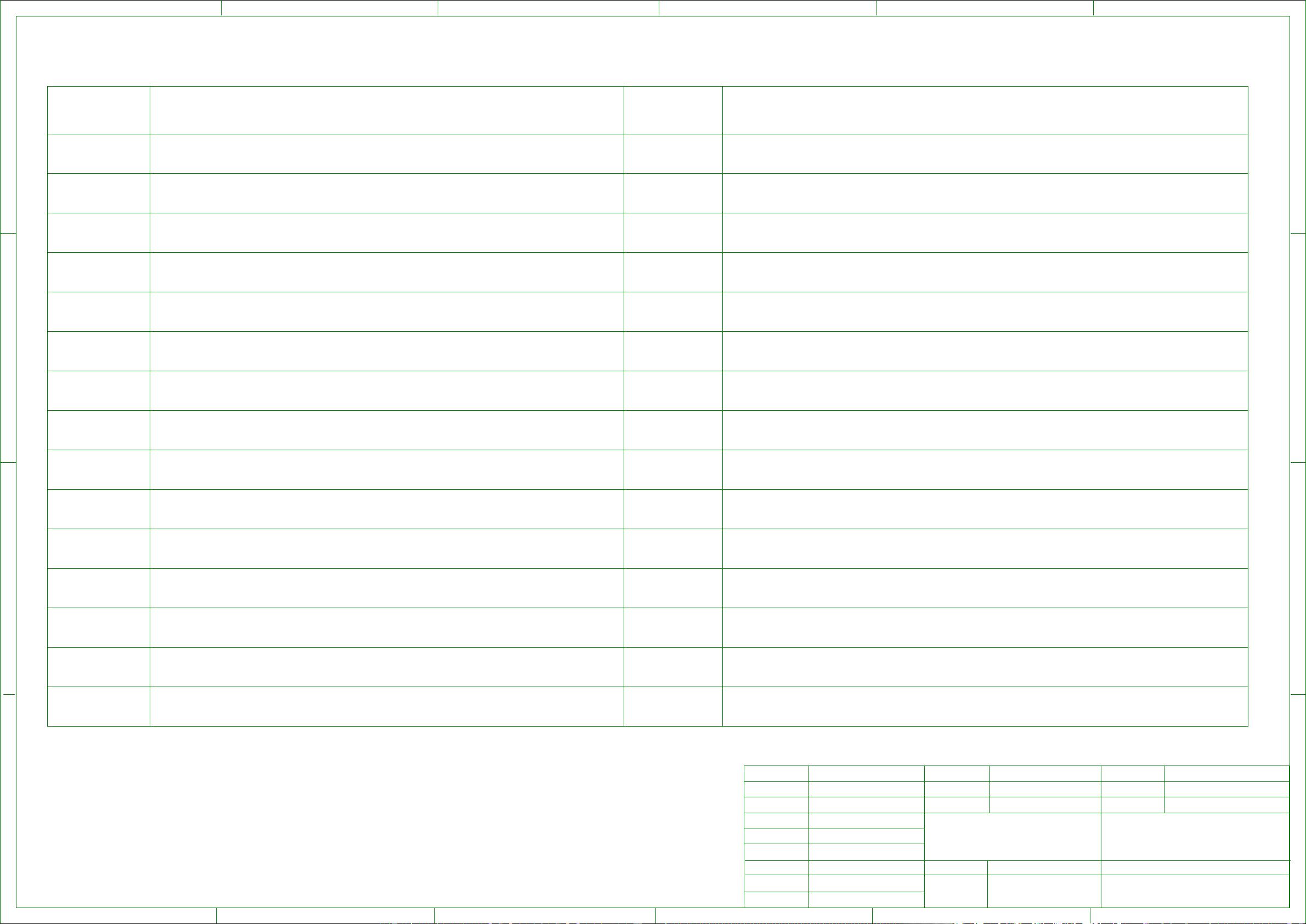
Change List
SCH update list
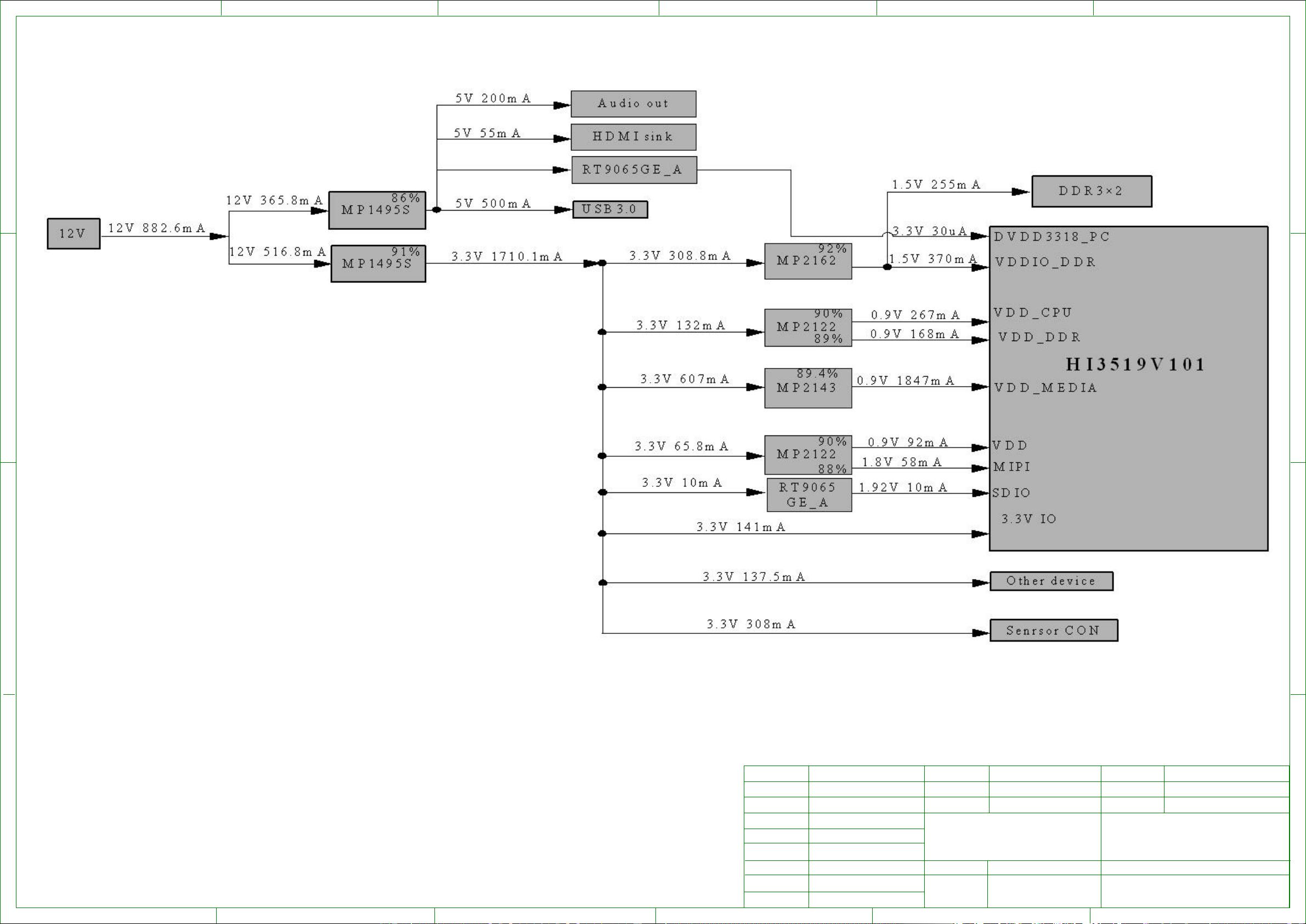
update the power tree in page 4.
change the netname from VO_DATA10 to VO_DATA10/PHY_CHIP_MODE in page 15.
add a pull down resistor of VO_DATA10/PHY_CHIP_MODE in page 15.
add "NOTES" in page 9 , page 15 and page 18.
update the symbol hi3519v101_per in page 15.move some SDIO signal out of the dotted line frame.6
7
8
9
10
add a LDO circuit only for DVDD18_SDIO(PIN L19) in page 9 and page 18.
change the external reset soc U6 from PT7M7809 to ADM706 in page 14.PT7M7809 cannot identify
the 1us low-level reset signal sent from the chip.
update the external circuit parameter of 24M and RTC crystal.change the value of R20 from11
20ohm to 100ohm.change value of load capacitor from 27pf to 22pf.
implement SVB control on the combined power supply.
The VDD and DDR core power supplies are combined into one power supply. PWM0 is used to12
The C350 filter capacitor of VDDIO_CK is isolated from the system GND by using the bead13
LB26, and is reserved for debugging (whether to add this capacitor is to be determined
based on the test result).
14
15 U31 is changed from the original dual-channel DC-DC MP2122 to single-channel MP2162.
the RESET system is defaulted to use POR mode in page 14.
The 1uF grounding filter capacitors C15 C118 are added to SDIO0_VOUT and SDIO1_VOUT.
update the package of U25 (HDMI PHY SII9136).
16
17
delete two TVS diode D12 D13.
isolate the PGND of ETH to GND of system using C204.
change the package name of U25.add many capacitors for power of U25.add C274 C273 C250 C206
C275 C276 for 1V2D_SII9136,add C277 C278 C279 C280 C281 C282 FOR 1V2A_SII9136,add C285 C284
C283 C287 C286 for IO3V3_SII9136 in page 21.
B 03030001
HI3519V101DMEB
HUZHENGWEN 292880
LISI XXXXX
2
NA
00001234
28


