没有合适的资源?快使用搜索试试~ 我知道了~
高精度角度传感器自动标定系统.pdf
1.该资源内容由用户上传,如若侵权请联系客服进行举报
2.虚拟产品一经售出概不退款(资源遇到问题,请及时私信上传者)
版权申诉
0 下载量 9 浏览量
2022-07-03
23:00:08
上传
评论
收藏 376KB PDF 举报
温馨提示
试读
26页
高精度角度传感器自动标定系统.pdf
资源推荐
资源详情
资源评论
TLC5618, TLC5618A
PROGRAMMABLE DUAL 12-BIT DIGITAL-TO-ANALOG CONVERTERS
SLAS156E – JULY 1997 – REVISED SEPTEMBER 1999
1
POST OFFICE BOX 655303 • DALLAS, TEXAS 75265
D
Programmable Settling Time to 0.5 LSB
2.5 µs or 12.5 µs Typ
D
Two 12-Bit CMOS Voltage Output DACs in
an 8-Pin Package
D
Simultaneous Updates for DAC A and
DAC B
D
Single Supply Operation
D
3-Wire Serial Interface
D
High-Impedance Reference Inputs
D
Voltage Output Range ... 2 Times the
Reference Input Voltage
D
Software Powerdown Mode
D
Internal Power-On Reset
D
TMS320 and SPI Compatible
D
Low Power Consumption:
3 mW Typ in Slow Mode,
8 mW Typ in Fast Mode
D
Input Data Update Rate of 1.21 MHz
D
Monotonic Over Temperature
D
Available in Q-Temp Automotive
HighRel Automotive Applications
Configuration Control / Print Support
Qualification to Automotive Standards
applications
D
Battery Powered Test Instruments
D
Digital Offset and Gain Adjustment
D
Battery Operated/Remote Industrial
Controls
D
Machine and Motion Control Devices
D
Cellular Telephones
description
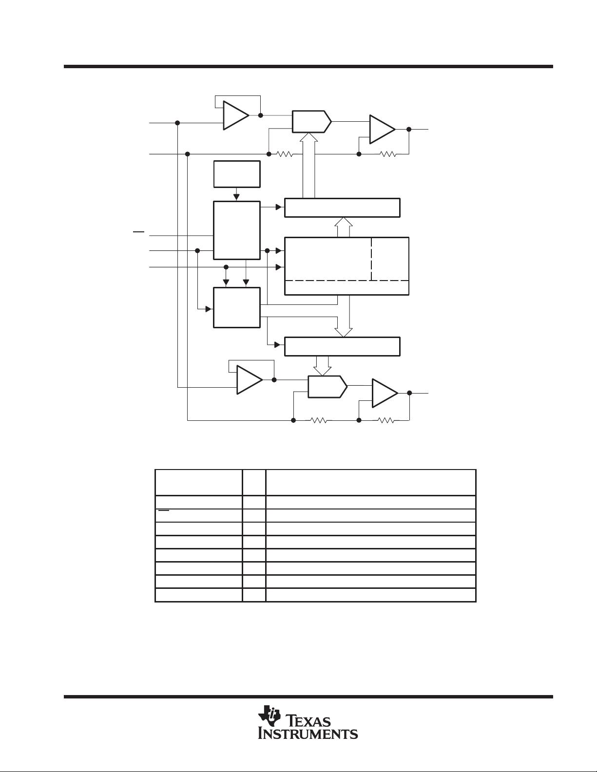
The TLC5618 is a dual 12-bit voltage output
digital-to-analog converter (DAC) with buffered
reference inputs (high impedance). The DACs
have an output voltage range that is two times the
reference voltage, and the DACs are monotonic.
The device is simple to use, running from a single
supply of 5 V. A power-on reset function is
incorporated in the device to ensure repeatable
start-up conditions.
Digital control of the TLC5618 is over a 3-wire
CMOS-compatible serial bus. The device re-
ceives a 16-bit word for programming and
producing the analog output. The digital inputs
feature Schmitt triggers for high noise immunity.
Digital communication protocols include the
SPI, QSPI, and Microwire standards.
Two versions of the device are available. The
TLC5618 does not have an internal state machine
and is dependent on all external timing signals. The TLC5618A has an internal state machine that counts the
number of clocks from the falling edge of CS
and then updates and disables the device from accepting further
data inputs. The TLC5618A is recommended for TMS320 and SPI processors, and the TLC5618 is
recommended only for SPI or 3-wire serial port processors. The TLC5618A is backward-compatible and
designed to work in TLC5618 designed systems.
Please be aware that an important notice concerning availability, standard warranty, and use in critical applications of
Texas Instruments semiconductor products and disclaimers thereto appears at the end of this data sheet.
SPI and QSPI are trademarks of Motorola, Inc.
Microwire is a trademark of National Semiconductor Corporation.
Copyright 1999, Texas Instruments Incorporated
PRODUCTION DATA information is current as of publication date.
Products conform to specifications per the terms of Texas Instruments
standard warranty. Production processing does not necessarily include
testing of all parameters.
1
2
3
4
8
7
6
5
DIN
SCLK
CS
OUT A
V
DD
OUT B
REFIN
AGND
D, P, OR JG PACKAGE
(TOP VIEW)
1920132
17
18
16
15
14
1312119 10
5
4
6
7
8
NC
OUTB
NC
REFIN
NC
NC
SCLK
NC
CS
NC
NC
DIN
NC
V
NC
OUTA
NC
AGND
NC
NC
FK PACKAGE
(TOP VIEW)
DD
On products compliant to MIL-PRF-38535, all parameters are tested
unless otherwise noted. On all other products, production
processing does not necessarily include testing of all parameters.
TLC5618, TLC5618A
PROGRAMMABLE DUAL 12-BIT DIGITAL-TO-ANALOG CONVERTERS
SLAS156E – JULY 1997 – REVISED SEPTEMBER 1999
2
POST OFFICE BOX 655303 • DALLAS, TEXAS 75265
description (continued)
The 8-terminal small-outline D package allows digital control of analog functions in space-critical applications.
The TLC5618C is characterized for operation from 0°C to 70°C. The TLC5618I is characterized for operation
from –40°C to 85°C. The TLC5618Q is characterized for operation from –40°C to 125°C. The TLC5618M is
characterized for operation from –55°C to 125°C.
AVAILABLE OPTIONS
PACKAGE
T
A
SMALL OUTLINE
†
(D)
PLASTIC DIP
(P)
CERAMIC DIP
(JG)
20 PAD LCC
(FK)
0°C to 70°C
TLC5618CD
TLC5618ACD
TLC5618CP
TLC5618ACP
—
—
—
—
–40°C to 85°C
TLC5618ID
TLC5618AID
TLC5618IP
TLC5618AIP
—
—
—
—
–40°C to 125°C TLC5618AQD — — —
–55°C to 125°C — — TLC5618AMJG TLC5618AMFK
†
The D package is available in tape and reel by adding R to the part number
(e.g., TLC5618CDR)
DEVICE
COMPATIBILITY
TLC5618 SPI, QSPI and Microwire
TLC5618A TMS320Cxx, SPI, QSPI, and Microwire
TLC5618, TLC5618A
PROGRAMMABLE DUAL 12-BIT DIGITAL-TO-ANALOG CONVERTERS
SLAS156E – JULY 1997 – REVISED SEPTEMBER 1999
3
POST OFFICE BOX 655303 • DALLAS, TEXAS 75265
functional block diagram
_
+
DAC
12-Bit DAC Register Latch A
Power-Up
Reset
Control
Logic
16-Bit Shift Register
4
Program
Bits
12 Data Bits
(LSB) (MSB)
REFIN
AGND
CS
SCLK
DIN
OUT A
(Voltage Output)
_
+
RR
DAC A
×2
Double
Buffer
Latch
_
+
_
+
OUT B
(Voltage Output)
DAC B
DAC
R
×2
R
12-Bit DAC Register Latch B
7
4
6
5
3
2
1
Terminal Functions
TERMINAL
I/O
DESCRIPTION
NAME NO.
I/O
DESCRIPTION
AGND 5 Analog ground
CS 3 I Chip select, active low
DIN 1 I Serial data input
OUT A 4 O DAC A analog output
OUT B 7 O DAC B analog output
REFIN 6 I Reference voltage input
SCLK 2 I Serial clock input
V
DD
8 Positive power supply
TLC5618, TLC5618A
PROGRAMMABLE DUAL 12-BIT DIGITAL-TO-ANALOG CONVERTERS
SLAS156E – JULY 1997 – REVISED SEPTEMBER 1999
4
POST OFFICE BOX 655303 • DALLAS, TEXAS 75265
absolute maximum ratings over operating free-air temperature range (unless otherwise noted)
†
Supply voltage (V
DD
to AGND) 7 V. . . . . . . . . . . . . . . . . . . . . . . . . . . . . . . . . . . . . . . . . . . . . . . . . . . . . . . . . . . . . . .
Digital input voltage range to AGND – 0.3 V to V
DD
+ 0.3 V. . . . . . . . . . . . . . . . . . . . . . . . . . . . . . . . . . . . . . . . . .
Reference input voltage range to AGND – 0.3 V to V
DD
+ 0.3 V. . . . . . . . . . . . . . . . . . . . . . . . . . . . . . . . . . . . . .
Output voltage at OUT from external source V
DD
+ 0.3 V. . . . . . . . . . . . . . . . . . . . . . . . . . . . . . . . . . . . . . . . . . . .
Continuous current at any terminal ±20 mA. . . . . . . . . . . . . . . . . . . . . . . . . . . . . . . . . . . . . . . . . . . . . . . . . . . . . . . .
Operating free-air temperature range, T
A
: TLC5618C, TLC5618AC 0°C to 70°C. . . . . . . . . . . . . . . . . . . . . . . .
TLC5618I, TLC5618AI –40°C to 85°C. . . . . . . . . . . . . . . . . . . . . . .
TLC5618AQ –40°C to 125°C. . . . . . . . . . . . . . . . . . . . . . . . . . . . . . .
TLC5618AM –55°C to 125°C. . . . . . . . . . . . . . . . . . . . . . . . . . . . . . .
Storage temperature range, T
stg
–65°C to 150°C. . . . . . . . . . . . . . . . . . . . . . . . . . . . . . . . . . . . . . . . . . . . . . . . . . .
Lead temperature 1,6 mm (1/16 inch) from case for 10 seconds 260°C. . . . . . . . . . . . . . . . . . . . . . . . . . . . . . .
†
Stresses beyond those listed under “absolute maximum ratings” may cause permanent damage to the device. These are stress ratings only, and
functional operation of the device at these or any other conditions beyond those indicated under “recommended operating conditions” is not
implied. Exposure to absolute-maximum-rated conditions for extended periods may affect device reliability.
DISSIPATION RATING TABLE
PACKAGE
T
A
≤ 25°C DERATING FACTOR T
A
= 70°C T
A
= 85°C T
A
= 125°C
PACKAGE
A
POWER RATING ABOVE T
A
= 25°C
‡
A
POWER RATING
A
POWER RATING
A
POWER RATING
D 635 mW 5.08 mW/°C 407 mW 330 mW —
FK 1375 mW 11.00 mW/°C 880 mW 715 mW 275 mW
JG 1050 mW 8.40 mW/°C 672 mW 546 mW 210 mW
P 1202 mW 9.61 mW/°C 769 mW 625 mW —
‡
This is the inverse of the traditional Junction-to-Ambient thermal Resistance (RΘ
JA
). Thermal Resistances are not production tested and are for
informational purposes only.
recommended operating conditions
MIN NOM MAX UNIT
Supply voltage, V
DD
4.5 5 5.5 V
High-level digital input voltage, V
IH
V
DD
= 5 V 0.7 V
DD
V
Low-level digital input voltage, V
IL
V
DD
= 5 V 0.3 V
DD
V
Reference voltage, V
ref
to REFIN terminal 2 2.048 V
DD
–1.1 V
Load resistance, R
L
2 kΩ
TLC5618C, TLC5618AC 0 70
O
p
erating free air tem
p
erature T
A
TLC5618I, TLC5618AI –40 85
°
C
Operating
free
-
air
temperat
u
re
,
T
A
TLC5618AQ –40 125
°C
TLC5618AM –55 125
TLC5618, TLC5618A
PROGRAMMABLE DUAL 12-BIT DIGITAL-TO-ANALOG CONVERTERS
SLAS156E – JULY 1997 – REVISED SEPTEMBER 1999
5
POST OFFICE BOX 655303 • DALLAS, TEXAS 75265
electrical characteristics over recommended operating free-air temperature range, V
DD
= 5 V ±5%,
V
ref(REFIN)
= 2.048 V (unless otherwise noted)
static DAC specifications
PARAMETER TEST CONDITIONS MIN TYP MAX UNIT
Resolution 12 bits
Integral nonlinearity (INL), end point adjusted V
ref(REFIN)
= 2.048 V, See Note 1 ±4 LSB
Differential nonlinearity (DNL) V
ref(REFIN)
= 2.048 V, See Note 2 ±0.5 ± 1 LSB
E
ZS
Zero-scale error (offset error at zero scale) V
ref(REFIN)
= 2.048 V, See Note 3 ±12 mV
Zero-scale-error temperature coefficient V
ref(REFIN)
= 2.048 V, See Note 4 3 ppm/°C
E
G
Gain error V
ref(REFIN)
= 2.048 V, See Note 5 ±0.29
% of FS
voltage
Gain error temperature coefficient V
ref(REFIN)
= 2.048 V, See Note 6 1 ppm/°C
Zero scale
Slow
65
PSRR
Power-su
pp
ly rejection ratio
Gain
See Notes 7 and 8
Slo
w
65
dB
PSRR
Power
-
su ly
rejection
ratio
Zero scale
See
Notes
7
and
8
Fast
65
dB
Gain
Fast
65
NOTES: 1. The relative accuracy or integral nonlinearity (INL) sometimes referred to as linearity error, is the maximum deviation of the output
from the line between zero and full scale excluding the effects of zero code and full-scale errors.
2. The differential nonlinearity (DNL) sometimes referred to as differential error, is the difference between the measured and ideal 1
LSB amplitude change of any two adjacent codes. Monotonic means the output voltage changes in the same direction (or remains
constant) as a change in the digital input code.
3. Zero-scale error is the deviation from zero voltage output when the digital input code is zero.
4. Zero-scale-error temperature coefficient is given by: E
ZS
TC = [E
ZS
(T
max
) – E
ZS
(T
min
)]/V
ref
× 10
6
/(T
max
– T
min
).
5. Gain error is the deviation from the ideal output (V
ref
– 1 LSB) with an output load of 10 kΩ excluding the effects of the zero-error.
6. Gain temperature coefficient is given by: E
G
TC = [E
G
(T
max
) – E
G
(T
min
)]/V
ref
× 10
6
/(T
max
– T
min
).
7. Zero-scale-error rejection ratio (EZS-RR) is measured by varying the V
DD
from 4.5 V to 5.5 V dc and measuring the proportion of
this signal imposed on the zero-code output voltage.
8. Gain-error rejection ratio (EG-RR) is measured by varying the V
DD
from 4.5 V to 5.5 V dc and measuring the proportion of this signal
imposed on the full-scale output voltage after subtracting the zero scale change.
OUT A and OUT B output specifications
PARAMETER TEST CONDITIONS MIN TYP MAX UNIT
V
O
Voltage output range R
L
= 10 kΩ 0 V
DD
–0.4 V
Output load regulation accuracy V
O(OUT)
= 4.096 V, R
L
= 2 kΩ ±0.29
% of FS
voltage
I
OSC(sink)
Out
p
ut short circuit sink current
V
O(A
OUT)
= V
DD
,
V
O(B OUT)
=V
DD
Fast 38
mA
I
OSC(
s
i
n
k)
Out ut
short
circuit
sink
current
V
O(B
OUT)
=
V
DD
,
Input code zero
Slow 23
mA
I
OSC(source)
Out
p
ut short circuit source current
V
O(A
OUT)
= 0 V,
V
O(B OUT)
=0V
Fast –54
mA
I
OSC(
source
)
Out ut
short
circuit
source
current
V
O(B
OUT)
=
0
V
,
Full-scale code
Slow –29
mA
I
O(sink)
Output sink current V
O(OUT)
= 0.25 V 5 mA
I
O(source)
Output source current V
O(OUT)
= 4.2 V 5 mA
剩余25页未读,继续阅读
资源评论
书博教育
- 粉丝: 1
- 资源: 2835
上传资源 快速赚钱
- 我的内容管理 展开
- 我的资源 快来上传第一个资源
- 我的收益 登录查看自己的收益
- 我的积分 登录查看自己的积分
- 我的C币 登录后查看C币余额
- 我的收藏
- 我的下载
- 下载帮助
安全验证
文档复制为VIP权益,开通VIP直接复制
信息提交成功