没有合适的资源?快使用搜索试试~ 我知道了~
温馨提示
试读
147页
1.0功能 -不支持的功能:大扇区大小(4KB) <Common> 工作温度:-25C~85C 包装:221球FBGA型-11.5毫米x13毫米x1.0毫米 0.5毫米球距 <e.MMC> •嵌入式多媒体卡。5.0兼容。详细描述如下: 参照JEDEC标准 •三星e·MMC支持eMMC5的功能。已定义的0 在JEDEC标准中 -支持的功能:压缩命令、缓存、丢弃、清理、, 断电通知、数据标记、分区类型、上下文ID、, 实时时钟,动态设备容量,HS200,HS400, 现场固件更新。 •与以前的多媒体卡系统完全向后兼容 规格(1位数据总线、多e·MMC系统) •数据总线宽度:1位(默认)、4位和8位 •MMC I/F时钟频率:0~200MHz •MMC I/F启动频率:0~52MHz •电源:接口电源→ VDD(VCCQ)(1.70V~1.95V或2.7V~ 3.6V),存储电源→ VDDF(VCC)(2.7V~3.6V) <LPDDR3 SDRAM> •双数据速率架构;每个时钟周期两次数据传输 •双向数据选通(DQS_t,DQS_
资源详情
资源评论
资源推荐
- 1 -
KMQ310006A-B419
Rev. 1.0, Mar. 2015
SAMSUNG ELECTRONICS RESERVES THE RIGHT TO CHANGE PRODUCTS, INFORMATION AND
SPECIFICATIONS WITHOUT NOTICE.
Products and specifications discussed herein are for reference purposes only. All information discussed
herein is provided on an "AS IS" basis, without warranties of any kind.
This document and all information discussed herein remain the sole and exclusive property of Samsung
Electronics. No license of any patent, copyright, mask work, trademark or any other intellectual property
right is granted by one party to the other party under this document, by implication, estoppel or other-
wise.
Samsung products are not intended for use in life support, critical care, medical, safety equipment, or
similar applications where product failure could result in loss of life or personal or physical harm, or any
military or defense application, or any governmental procurement to which special terms or provisions
may apply.
For updates or additional information about Samsung products, contact your nearest Samsung office.
All brand names, trademarks and registered trademarks belong to their respective owners.
© 2015 Samsung Electronics Co., Ltd. All rights reserved.
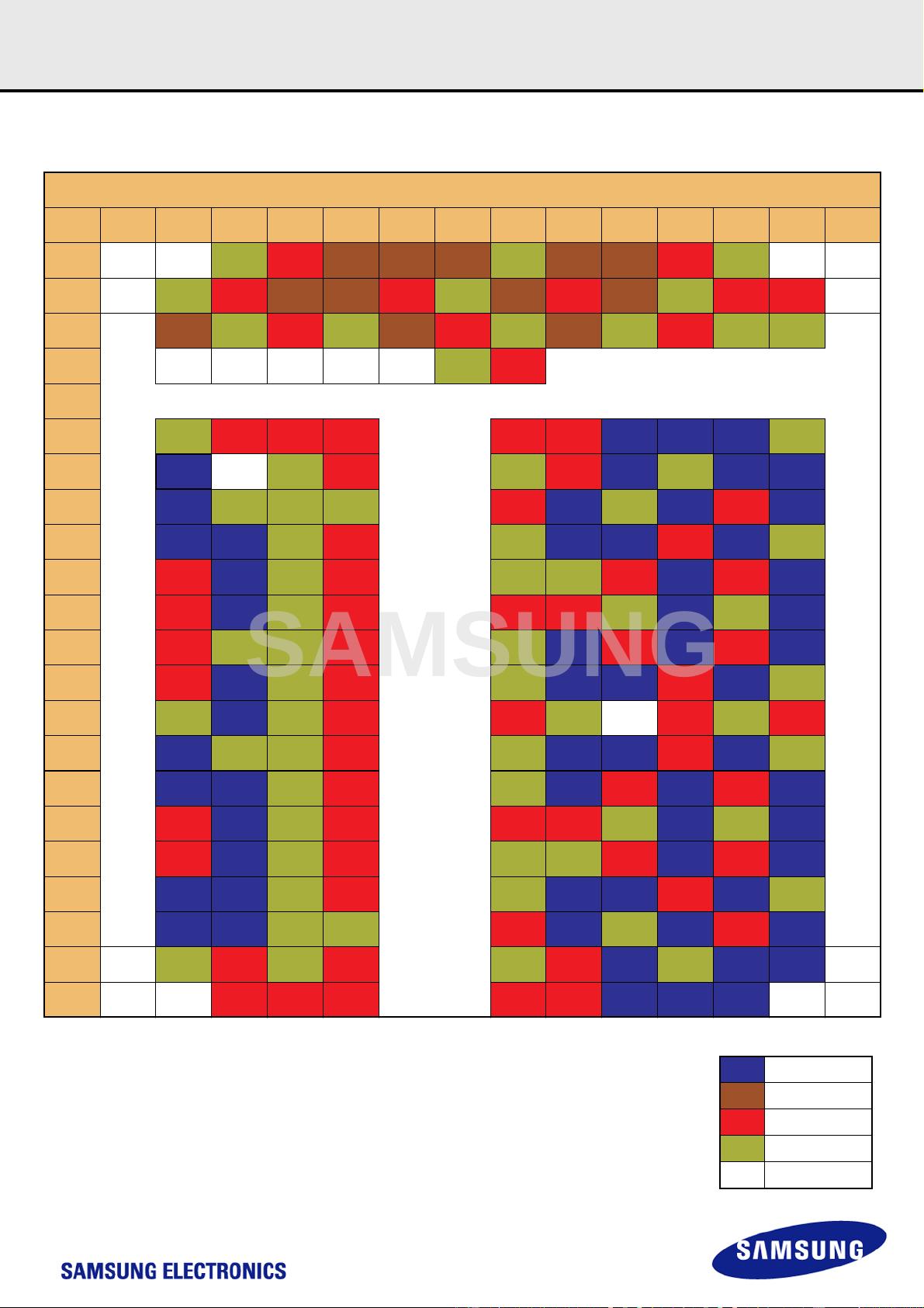
MCP Specification
221FBGA, 11.5x13x1.0mmt
16GB e.MMC + 12Gb(6Gb*2) DDP LPDDR3 SDRAM
datasheet
SAMSUNG
- 2 -
KMQ310006A-B419 MCP Memory
Rev. 1.0
datasheet
Revision History
Revision No. History Draft Date Remark Editor
0.0 Initial issue.
- 16GB e.MMC D-die R11
- 12Gb(6Gb*2) LPDDR3 SDRAM A-die R10
5th Dec, 2014 Preliminary B.Jeong
1.0 Final datasheet.
<e.MMC>
• None
<LPDDR3>
• 12Gb(6Gb*2) LPDDR3 SDRAM A-die R11 update
• Correct errata.
4th Mar, 2015 Final B.Jeong
SAMSUNG
- 3 -
KMQ310006A-B419 MCP Memory
Rev. 1.0
datasheet
1.0 FEATURES
- Non-supported Features : Large Sector Size (4KB)
<Common>
Operating
Temperature : -25C ~ 85C
Package : 221Ball FBGA Type - 11.5mm x 13mm x 1.0mmt
0.5mm ball pitch
<e.MMC>
•embedded MultiMediaCard Ver. 5.0 compatible. Detail description is
referenced by JEDEC Standard
•SAMSUNG e·MMC supports features of eMMC5.0 which are defined
in JEDEC Standard
- Supported Features : Packed command, Cache, Discard, Sanitize,
Power Off Notification, Data Tag, Partition types, Context ID,
Real Time Clock, Dynamic Device Capacity, HS200, HS400,
Field Firmware Update.
• Full backward compatibility with previous MultiMediaCard system
specification (1bit data bus, multi-e·MMC systems)
• Data bus width : 1bit (Default), 4bit and 8bit
• MMC I/F Clock Frequency : 0 ~ 200MHz
• MMC I/F Boot Frequency : 0 ~ 52MHz
• Power : Interface power → VDD(VCCQ) (1.70V ~ 1.95V or 2.7V ~
3.6V) , Memory power → VDDF(VCC) (2.7V ~ 3.6V)
<LPDDR3 SDRAM>
• Double-data rate architecture; two data transfers per clock cycle
• Bidirectional data strobes (DQS_t, DQS_c), These are transmitted/
received with data to be used in capturing data at the receiver
• Differential clock inputs (CK_t and CK_c)
• Differential data strobes (DQS_t and DQS_c)
• Commands & addresses entered on both positive and negative CK
edges; data and data mask referenced to both edges of DQS
• 8 internal banks for concurrent operation
• Data mask (DM) for write data
• Burst Length: 8
• Burst Type: Sequential
• Read & Write latency : Refer to Table 45 LPDDR3 AC Timing Table
• Auto Precharge option for each burst access
• Configurable Drive Strength
• All Bank Refresh, Per Bank Refresh and Self Refresh
• Partial Array Self Refresh and Temperature Compensated Self
Refresh
• Write Leveling
• CA Calibration
• HSUL_12 compatible inputs
• VDD1/VDD2/VDDQ/VDDCA
: 1.8V/1.2V/1.2V / 1.2V
• No DLL : CK to DQS is not synchronized
• Edge aligned data output, center aligned data input
• 2/CS, 2CKE
• On Die Termination using ODT pin
[Table 1] LPDDR3 SDRAM Addressing
NOTE :
1) The least-significant column address C0 is not transmitted on the CA bus, and is
implied to be zero.
2) t
REFI
values for all bank refresh is Tc = -25~85C, Tc means Operating Case Tem-
perature
3) Row and Column Address values on the CA bus that are not used are “don’t care.”
4) No memory present at addresses with R13=R14=HIGH. ACT command with
R13=R14=HIGH is ignored (NOP). Write to R13=R14=HIGH is ignored (NOP).
Items 6Gb
Number of Banks 8
Bank Addresses BA0-BA2
t
REFI
(us)
2)
3.9
×32
Row Addresses
3)
R0-R14
4)
Column Addresses
1), 3)
C0-C9
SAMSUNG
- 4 -
KMQ310006A-B419 MCP Memory
Rev. 1.0
datasheet
2.0 GENERAL DESCRIPTION
The KMQ310006A is a Multi Chip Package Memory which combines 16GB e.MMC and 12Gb(6Gb*2) DDP LPDDR3 SDRAM.
SAMSUNG e·MMC is an embedded MMC solution designed in a BGA package form. e·MMC operation is identical to a MMC device and therefore is a
simple read and write to memory using MMC protocol v5.0 which is a industry standard.e·MMC consists of NAND flash and a MMC controller. 3V supply
voltage is required for the NAND area (VDDF or VCC) whereas 1.8V or 3V dual supply voltage (VDD or VCCQ) is supported for the MMC controller. SAM-
SUNG e•MMC supports 200MHz DDR – up to 400MBps with bus widths of 8 bit in order to improve sequential bandwidth, especially sequential read per-
formance.There are several advantages of using e·MMC. It is easy to use as the MMC interface allows easy integration with any microprocessor with
MMC host. Any revision or amendment of NAND is invisible to the host as the embedded MMC controller insulates NAND technology from the host. This
leads to faster product development as well as faster times to market.The embedded flash management software or FTL(Flash Transition Layer) of
e·MMC manages Wear Leveling, Bad Block Management and ECC. The FTL supports all features of the Samsung NAND flash and achieves optimal per-
formance.
LPDDR3 devices use a double data rate architecture on the Command/Address (CA) bus to reduce the number of input pins in the system. The 10-bit CA
bus contains command, address, and bank information. Each command uses one clock cycle, during which command information is transferred on both
the positive and negative edge of the clock.
These devices also use a double data rate architecture on the DQ pins to achieve high speed operation. The double data rate architecture is essentially
an 8n prefetch architecture with an interface designed to transfer two data bits per DQ every clock cycle at the I/O pins. A single read or write access for
the LPDDR3 SDRAM effectively consists of a single 8n-bit wide, one clock cycle data transfer at the internal DRAM core and eight corresponding n-bit
wide, one-half-clock-cycle data transfers at the I/O pins.
Read and write accesses to the LPDDR3 SDRAMs are burst oriented; accesses start at a selected location and continue for a programmed number of
locations in a programmed sequence. Accesses begin with the registration of an Activate command, which is then followed by a Read or Write command.
The address and BA bits registered coincident with the Activate command are used to select the row and the Bank to be accessed. The address bits
registered coincident with the Read or Write command are used to select the Bank and the starting column location for the burst access.
Prior to normal operation, the LPDDR3 SDRAM must be initialized. The following section provides detailed information covering device initialization,
register definition, command description and device operation.
The KMQ310006A suitable for use in data memory of mobile communication system to reduce not only mount area but also power consumption. This
device is available in 221-ball FBGA Type.
SAMSUNG
- 5 -
KMQ310006A-B419 MCP Memory
Rev. 1.0
datasheet
3.0 PIN CONFIGURATION
221Ball FBGA
1 2 3 4 5 6 7 8 9 10 11 12 13 14
A
DNU VSF VSS_m VCCQ_m DAT6_m CMD_m RCLK_m VSS_m DAT0_m DAT5_m VDDl_m VSS_m VSF DNU
B
VSF VSS_m VCC_m DAT7_m DAT3_m VCCQ_m VSS_m CLK_m VCCQ_m DAT1_m VSS_m VCC_m VCC_m VSF
C
RST_m VSS_m VCC_m VSS_m DAT2_m VCCQ_m VSS_m DAT4_m VSS_m VCCQ_m VSS_m VSS_m
D
VSF VSF VSF VSF VSF VSS_m VCC_m
E
F
VSS_v VDD1_v VDD1_v VDD2_v VDD2_v VDD1_v DQ29_v DQ30_v DQ31_v VSSQ_v
G
ZQ_v NC VSS_v VDD1_v VSS_v VDDQ_v DQ26_v VSSQ_v DQ27_v DQ28_v
H
CA9_v VSS_v
VSS-
CA_v
VSS_v VDDQ_v
DQS3_t_
v
VSSQ_v DQ24_v VDDQ_v DQ25_v
J
CA8_v CA7_v
VSS-
CA_v
VDD2_v VSSQ_v
DQS3_c_
v
DM3_v VDDQ_v DQ15_v VSSQ_v
K
VDDCA_
v
CA6_v
VSS-
CA_v
VDD2_v VSSQ_v VSSQ_v VDDQ_v DQ13_v VDDQ_v DQ14_v
L
VDD2_v CA5_v VSS_v VDD2_v - - VDDQ_v VDDQ_v VSSQ_v DQ12_v VSSQ_v DQ11_v -
M
VREF-
CA_v
VSS_v VSS_v VDD2_v - - VSSQ_v
DQS1_t_
v
VDDQ_v DQ10_v VDDQ_v DQ9_v -
N
VDDCA_
v
CK_c_v VSS_v VDD2_v - - VSS_v
DQS1_c_
v
DM1_v VDDQ_v DQ8_v VSSQ_v -
P
VSS-
CA_v
CK_t_v VSS_v VDD2_v - - VDD2_v VSSQ_v DNU VDD2_v VSS_v
VREFD-
Q_v
-
R
CKE1_v VSS_v VSS_v VDD2_v - - VSS_v
DQS0_c_
v
DM0_v VDDQ_v DQ7_v VSSQ_v -
T
CKE0_v /CS1_v VSS_v VDD2_v - - VSSQ_v
DQS0_t_
v
VDDQ_v DQ5_v VDDQ_v DQ6_v -
U
VDDCA_
v
/CS0_v
VSS-
CA_v
VDD2_v - - VDDQ_v VDDQ_v VSSQ_v DQ3_v VSSQ_v DQ4_v -
V
VDDCA_
v
CA4_v
VSS-
CA_v
VDD2_v - - VSSQ_v VSSQ_v VDDQ_v DQ1_v VDDQ_v DQ2_v -
W
CA2_v CA3_v
VSS-
CA_v
VDD2_v - - VSSQ_v
DQS2_c_
v
DM2_v VDDQ_v DQ0_v VSSQ_v
Y
CA0_v CA1_v VSS_v VSS_v - - VDDQ_v
DQS2_t_
v
VSSQ_v DQ23_v VDDQ_v DQ22_v -
AA
DNU VSS_v VDD1_v VSS_v VDD1_v VSS_v VDDQ_v DQ21_v VSSQ_v DQ20_v DQ19_v DNU-
AB
DNU DNU VDD1_v VDD1_v VDD2_v VDD2_v VDD1_v DQ18_v DQ17_v DQ16_v DNU- DNU
221 FBGA: Top View (Ball Down)
LPDDR3
e.MMC
Power
Ground
DNU / VSF / NC
SAMSUNG
剩余146页未读,继续阅读
奇待
- 粉丝: 0
- 资源: 7
上传资源 快速赚钱
- 我的内容管理 展开
- 我的资源 快来上传第一个资源
- 我的收益 登录查看自己的收益
- 我的积分 登录查看自己的积分
- 我的C币 登录后查看C币余额
- 我的收藏
- 我的下载
- 下载帮助
安全验证
文档复制为VIP权益,开通VIP直接复制
信息提交成功
评论0