TL/F/5120
MM54HC138/MM74HC138 3-to-8 Line Decoder
January 1988
MM54HC138/MM74HC138
3-to-8 Line Decoder
General Description
This decoder utilizes advanced silicon-gate CMOS technol-
ogy, and is well suited to memory address decoding or data
routing applications. The circuit features high noise immuni-
ty and low power consumption usually associated with
CMOS circuitry, yet has speeds comparable to low power
Schottky TTL logic.
The MM54HC138/MM74HC138 has 3 binary select inputs
(A, B, and C). If the device is enabled these inputs deter-
mine which one of the eight normally high outputs will go
low. Two active low and one active high enables (G1, G2A
and G2B) are provided to ease the cascading of decoders.
The decoder’s outputs can drive 10 low power Schottky TTL
equivalent loads, and are functionally and pin equivalent to
the 54LS138/74LS138. All inputs are protected from dam-
age due to static discharge by diodes to V
CC
and ground.
Features
Y
Typical propagation delay: 20 ns
Y
Wide power supply range: 2V–6V
Y
Low quiescent current: 80 mA maximum (74HC Series)
Y
Low input current: 1 mA maximum
Y
Fanout of 10 LS-TTL loads
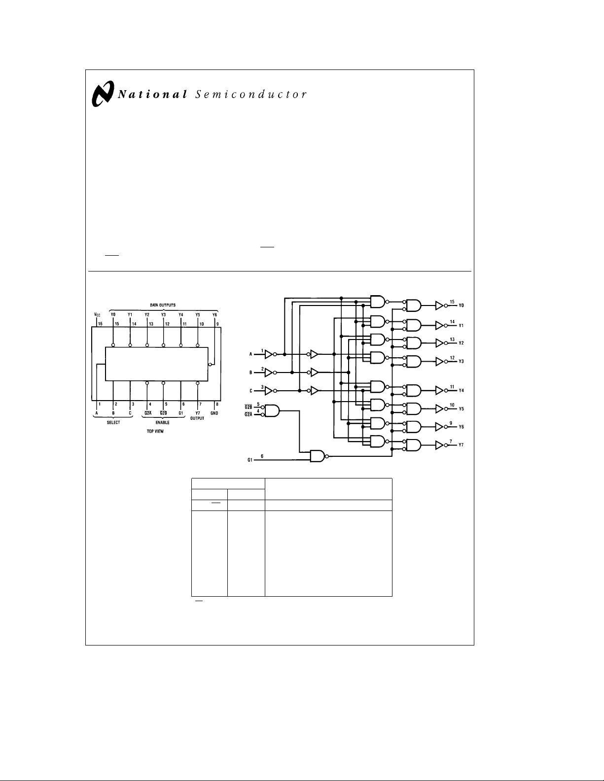
Connection and Logic Diagrams
Dual-In-Line Package
TL/F/5120–1
Order Number MM54HC138
or MM74HC138
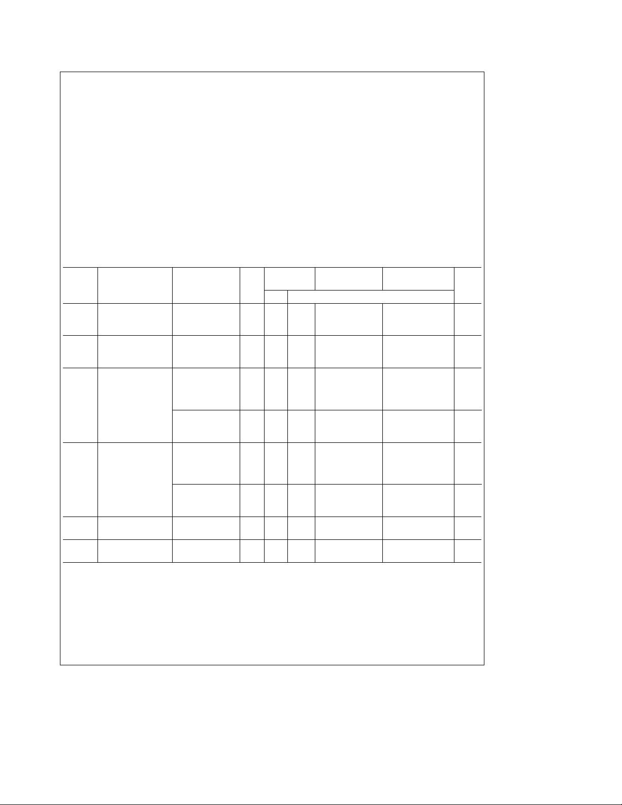
Truth Table
Inputs
Outputs
Enable Select
G1 G2* CBAY0Y1Y2Y3Y4Y5Y6Y7
X HXXXHHHHHHHH
L XXXXHHHHHHHH
H L LLLLHHHHHHH
H L LLHHLHHHHHH
H L LHLHHLHHHHH
H L LHHHHHLHHHH
H L HLLHHHHLHHH
H L HLHHHHHHLHH
H L HHLHHHHHHLH
H L HHHHHHHHHHL
*G2
e
G2A
a
G2B
H
e
high level, L
e
low level, X
e
don’t care
TL/F/5120–2
C
1995 National Semiconductor Corporation RRD-B30M105/Printed in U. S. A.