没有合适的资源?快使用搜索试试~ 我知道了~
ACT8846_Datasheet
需积分: 10 12 下载量 13 浏览量
2018-02-06
12:33:49
上传
评论
收藏 3.45MB PDF 举报
温馨提示
试读
43页
ACT8846_Datasheet 英文版,功能强大的PMU,可以作为平台级的供电方案选型
资源推荐
资源详情
资源评论
Innovative Power
TM
- 1 - www.active-semi.com
Copyright © 2016-2017 Active-Semi, Inc.
ActivePMU
TM
is a trademark of Active-Semi.
I
2
C
TM
is a trademark of NXP.
ACT8846
Advanced PMU for Multi-core Application Processors
FEATURES
INTEGRATED POWER SUPPLIES
Four DC/DC Step-Down (Buck) Regulators
2 x 2.8A, 2 x 1.5A
Five Low-Noise LDOs
2 x 150mA, 3 x 350mA
Three Low-Input Voltage LDOs
1 x 150mA, 2 x 350mA
One Low IQ Keep-Alive LDO
Backup Battery Charger
SYSTEM CONTROL AND INTERFACE
Four General Purpose I/O with PWM Drivers
I
2
C Serial Interface
Interrupt Controller
SYSTEM MANAGEMENT
Reset Interface and Sequencing Controller
Power on Reset
Soft / Hard Reset
Watchdog Supervision
Multiple Sleep Modes
Thermal Management Subsystem
APPLICATIONS
Tablet PC
Mobile Internet Devices (MID)
E-books
Personal Navigation Devices
Smart Phones
GENERAL DESCRIPTION
The ACT8846 is a complete, cost effective, and
highly-efficient ActivePMU
TM
power management
solution optimized for the power, voltage
sequencing and control requirements of Rockchip
RK31x8 application processor family.
The ACT8846 features four fixed-frequency,
current-mode, synchronous PWM step-down
converters that achieve peak efficiencies of up to
97%. These regulators operate with a fixed
frequency of 2.25MHz, minimizing noise in sensitive
applications and allowing the use of small external
components. These buck regulators supply up to
2.8A of output current and can fully satisfy the
power and control requirements of the multi-core
application processor. Dynamic Voltage Scaling
(DVS) is supported either by dedicated control pins,
or through I2C interface to optimize the energy-per-
task performance for the processor. This device
also include eight low-noise LDOs (up to 350mA
per LDO), one always-on LDO and an integrated
backup battery charger to provide a complete
power system for the processor.
The power sequence and reset controller provides
power-on reset, SW-initiated reset, and power cycle
reset for the processor. It also features the
watchdog supervisory function. Multiple sleep
modes with autonomous sleep and wake-up
sequence control are supported.
The thermal management and protection
subsystem allows the host processor to manage the
power dissipation of the PMU and the overall
system dynamically. The PMU provides a thermal
warning to the host processor when the
temperature reaches a certain threshold such that
the system can turn off some of the non-essential
functions, reduce the clock frequency and etc to
manage the system temperature.
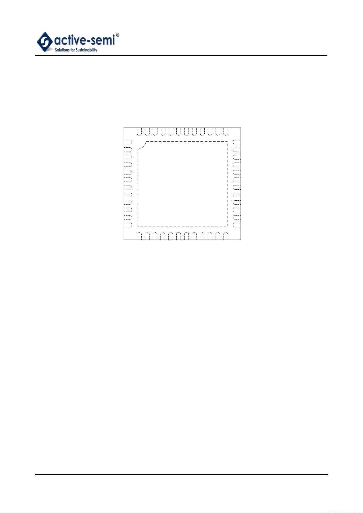
The ACT8846 is available in a compact, Pb-Free
and RoHS-compliant TQFN66-48 package.
Rev 5, 09-Mar-17
ACT8846
Rev 5, 09-Mar-17
Innovative Power
TM
- 2 - www.active-semi.com
Copyright © 2016-2017 Active-Semi, Inc.
ActivePMU
TM
is a trademark of Active-Semi.
I
2
C
TM
is a trademark of NXP.
SDA
REG2
VP2
GP2
SW2
OUT2
OUT2
REG1
VP1
GP14
SW1
OUT1
FB1
To Battery
nIRQ
REG5
LDO
OUT5
OUT5
INL1
REFBP
Reference
REG3
VP3
GP3
SW3
OUT3
OUT3
GA
EP
nPBSTAT
PWRHLD
PWREN
SCL
nRSTO
VSELR2
V
IO
nPBIN
PUSH BUTTON
INL2
REG6
LDO
OUT6
OUT6
REG7
LDO
OUT7
OUT7
REG10
LDO
OUT10
OUT10
To Battery
To Battery
REG4
VP4
GP14
SW4
OUT4
OUT4
To Battery
REG11
LDO
OUT11
OUT11
INL3
REG12
LDO
OUT12
OUT12
V
IO
V
IO
REG13
RTC LDO
OUT13
GPIO2
GPIO1
GPIO3
System
Control
INL2
REG8
LDO
OUT8
OUT8
REG9
LDO
OUT9
OUT9
OUT13
ACT8846
To Battery
To Battery
To Battery
GPIO4
GPIO6
GPIO5
FUNCTIONAL BLOCK DIAGRAM
ACT8846
Rev 5, 09-Mar-17
Innovative Power
TM
- 3 - www.active-semi.com
Copyright © 2016-2017 Active-Semi, Inc.
ActivePMU
TM
is a trademark of Active-Semi.
I
2
C
TM
is a trademark of NXP.
ORDERING INFORMATION
: All Active-Semi components are RoHS Compliant and with Pb-free plating unless specified differently. The term Pb-free means
semiconductor products that are in compliance with current RoHS (Restriction of Hazardous Substances) standards.
: Push button 10s shut down function is supported in ACT8846QM468-T and ACT8846QM490-T and ACT8846QM468-T15.
PART NUMBER V
OUT1
V
OUT2
V
OUT3
V
OUT4
V
OUT5
V
OUT6
V
OUT7
V
OUT8
V
OUT9
V
OUT10
V
OUT11
V
OUT12
V
OUT13
ACT8846QM460-T
Adjustable 1.0V 1.0V 3.0V 1.0V 1.2V 1.8V 3.3V 3.3V 3.3V 1.8V 2.8V 1.8V
ACT8846QM468-T
Adjustable 1.0V 1.0V 3.0V 1.0V 1.2V 1.8V 3.3V 3.3V 3.3V 1.8V 2.8V 1.8V
ACT8846QM490-T
1.2V 3.3V 1.1V 2.0V 3.3V 1.0V 3.3V 3.3V 3.3V 1.0V 1.8V 1.8V 1.8V
ACT8846QM468-T15
Adjustable 1.0V 1.0V 3.0V 1.0V 1.2V 1.8V 3.3V 3.3V 3.3V 1.8V 2.8V 1.8V
ACT8846QM102-T
1.45V 1.8V 1.1V 2.8V 2.5V 1.8V 2.5V 1.8V 3.3V 1.1V 3.3V 3.0V 1.8V
ACT8846QM_ _ _-T
Option Code
Pin Count
Package Code
Product Number
Tape and Reel
PACKAGE PINS TEMPERATURE RANGE
TQFN66-48 48
-40°C to +85°C
ACT8846
Rev 5, 09-Mar-17
Innovative Power
TM
- 4 - www.active-semi.com
Copyright © 2016-2017 Active-Semi, Inc.
ActivePMU
TM
is a trademark of Active-Semi.
I
2
C
TM
is a trademark of NXP.
PIN CONFIGURATION
TOP VIEW
Thin - QFN (TQFN66-48)
EP
OUT13
OUT7
GPIO4
OUT6
INL1
OUT5
GPIO3
GPIO2
GPIO1
OUT3
GPIO5
GPIO6
nIRQ
nRSTO
PWRHLD
nPBIN
VP1
FB1
SW1
GP14
SW3
SW3
GP3
OUT10
OUT11
INL3
OUT12
VSELR2
nPBSTAT
GP2
SCL
SDA
OUT4
GA
OUT9
INL2
REFBP
PWREN
OUT2
OUT8
VP3
VP3
SW2
SW2
VP2
VP2
SW4
VP4
ACTIVE
8846QM
DATE CODE
ACT8846
Rev 5, 09-Mar-17
Innovative Power
TM
- 5 - www.active-semi.com
Copyright © 2016-2017 Active-Semi, Inc.
ActivePMU
TM
is a trademark of Active-Semi.
I
2
C
TM
is a trademark of NXP.
PIN DESCRIPTIONS
PIN NAME DESCRIPTION
1, 2 SW3 Switch Node for REG3.
3 GP3
Power Ground for REG3. Connect GP14, GP2, GP3, and GA together at a single
point as close to the IC as possible.
4 OUT10 REG10 output. Bypass it to ground with a 2.2µF capacitor.
5 OUT11 REG11 output. Bypass it to ground with a 2.2µF capacitor.
6 INL3 Power input for REG10, REG11 and REG12.
7 OUT12 REG12 output. Bypass it to ground with a 2.2µF capacitor.
8 VSELR2
Output Voltage Selection for REG2. Drive to logic low to select default output voltage.
Drive to logic high to select secondary output voltage.
9 nPBSTAT
Active-Low Open-Drain Push-Button Status Output. nPBSTAT is asserted low
whenever the nPBIN is pushed, and is high-Z otherwise.
10 GP2
Power ground for REG2. Connect GP14, GP2, GP3, and GA together at a single
point as close to the IC as possible.
11, 12 SW2 Switch Node for REG2.
13, 14 VP2
Power input for REG2. Bypass to GP2 with a high quality ceramic capacitor placed as
close to the IC as possible.
15 OUT2 Output Voltage Sense for REG2.
16 PWREN
Power Enable Input for REG3. PWREN is functional only when PWRHLD is driven
high. Drive PWREN to a logic high to turn on the REG3. Drive PWREN to a logic low
to turn off the REG3.
17 REFBP
Reference Bypass. Connect a 0.047μF ceramic capacitor from REFBP to GA. This
pin is discharged to GA in shutdown.
18 INL2 Power Input for REG8, REG9.
19 OUT9 REG9 output. Bypass it to ground with a 2.2µF capacitor.
20 GA Analog Ground.
21 OUT4 Output voltage sense for REG4.
22 OUT8 REG8 output. Bypass it to ground with a 2.2µF capacitor.
23 SDA Data Input for I
2
C Serial Interface. Data is read on the rising edge of SCL.
24 SCL Clock Input for I
2
C Serial Interface.
25 VP4
Power input for REG4. Bypass to GP14 with a high quality ceramic capacitor placed
as close to the IC as possible.
剩余42页未读,继续阅读
资源评论
Makarov丶hao
- 粉丝: 0
- 资源: 7
上传资源 快速赚钱
- 我的内容管理 展开
- 我的资源 快来上传第一个资源
- 我的收益 登录查看自己的收益
- 我的积分 登录查看自己的积分
- 我的C币 登录后查看C币余额
- 我的收藏
- 我的下载
- 下载帮助
安全验证
文档复制为VIP权益,开通VIP直接复制
信息提交成功