没有合适的资源?快使用搜索试试~ 我知道了~
L78芯片资料
需积分: 16 1 下载量 126 浏览量
2016-01-18
19:16:12
上传
评论
收藏 229KB PDF 举报
温馨提示
试读
25页
关于L78系列芯片的资料,详细介绍了芯片各引脚的作用以及使用方法,是一个非常全面的资料。
资源推荐
资源详情
资源评论
L7800
SERIES
POSITIVE VOLTAGE REGULATORS
November 2000
■ OUTPUT CURRENT UP TO 1.5 A
■ OUTPUT VOLTAGESOF 5; 5.2; 6; 8; 8.5; 9;
12; 15; 18; 24V
■ THERMAL OVERLOADPROTECTION
■ SHORT CIRCUIT PROTECTION
■ OUTPUT TRANSITION SOA PROTECTION
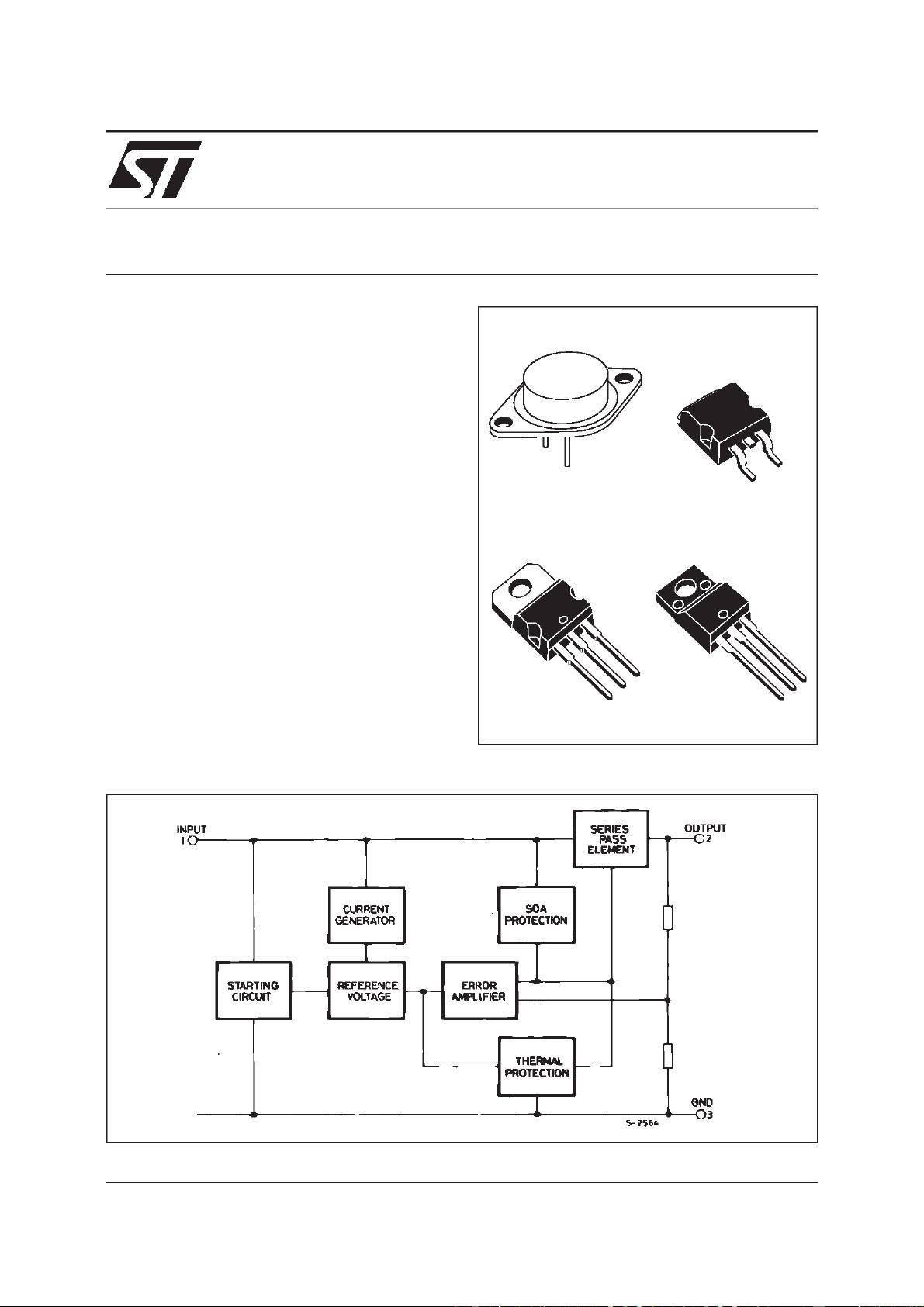
DESCRIPTION
The L7800 series of three-terminal positive
regulators is available in TO-220 TO-220FP TO-3
and D
2
PAK packages and several fixed output
voltages, making it useful in a wide range of
applications.These regulators can provide local
on-card regulation, eliminating the distribution
problems associated with single point regulation.
Each type employs internal current limiting,
thermal shut-down and safe area protection,
making it essentially indestructible. If adequate
heat sinking is provided, they can deliver over 1A
output current. Although designed primarily as
fixed voltage regulators, these devices can be
used with external components to obtain
adjustablevoltages and currents.
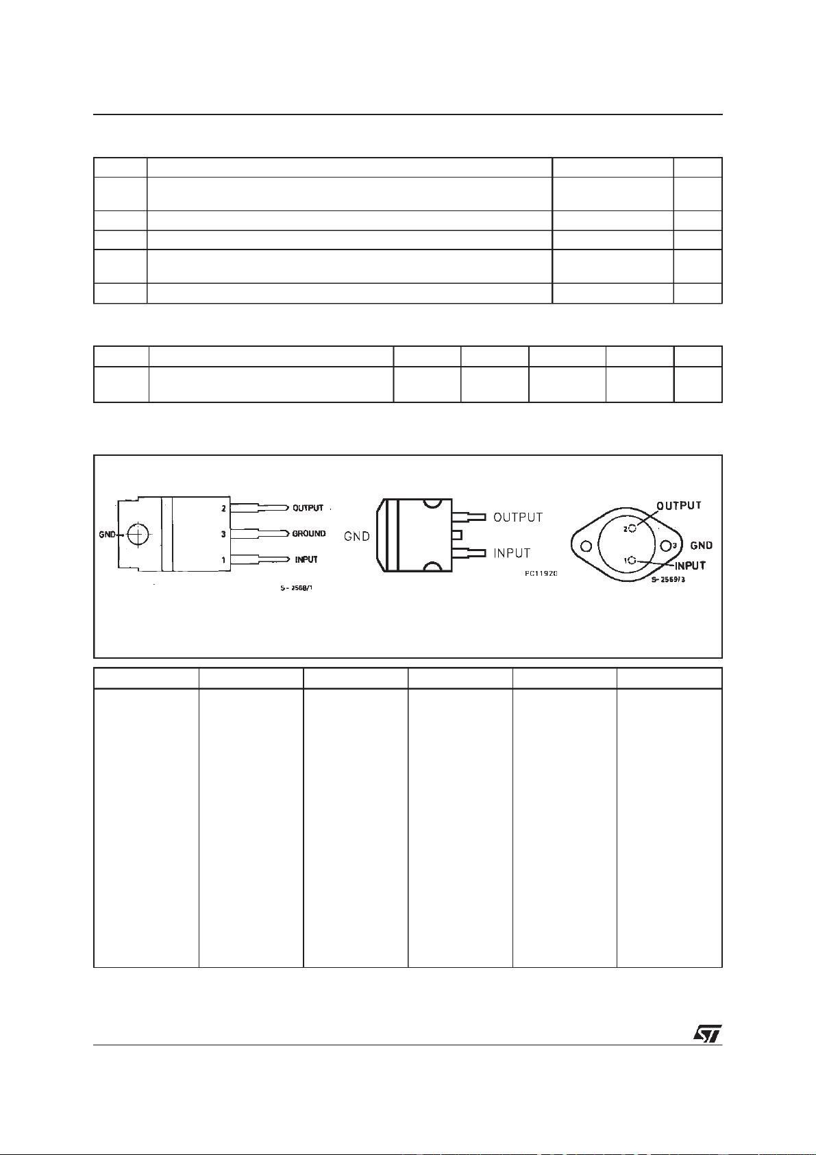
1
2
TO-3
TO-220 TO-220FP
D
2
PAK
BLOCK DIAGRAM
1/25
CONNECTION DIAGRAM AND ORDERING NUMBERS (top view)
TO-220 & TO-220FP TO-3D
2
PAK
THERMAL DATA
Symbol Parameter D
2
PAK TO-220 TO-220FP TO-3 Unit
R
thj-case
R
thj-amb
Thermal Resistance Junction-case Max
Thermal Resistance Junction-ambient Max
3
62.5
3
50
5
60
4
35
o
C/W
o
C/W
Type TO-220 D
2
PAK (*) TO-220FP TO-3 Output Voltage
L7805
L7805C
L7852C
L7806
L7806C
L7808
L7808C
L7885C
L7809C
L7812
L7812C
L7815
L7815C
L7818
L7818C
L7820
L7820C
L7824
L7824C
L7805CV
L7852CV
L7806CV
L7808CV
L7885CV
L7809CV
L7812CV
L7815CV
L7818CV
L7820CV
L7824CV
L7805CD2T
L7852CD2T
L7806CD2T
L7808CD2T
L7885CD2T
L7809CD2T
L7812CD2T
L7815CD2T
L7818CD2T
L7820CD2T
L7824CD2T
L7805CP
L7852CP
L7806CP
L7808CP
L7885CP
L7809CP
L7812CP
L7815CP
L7818CP
L7820CP
L7824CP
L7805T
L7805CT
L7852CT
L7806T
L7806CT
L7808T
L7808CT
L7885CT
L7809CT
L7812T
L7812CT
L7815T
L7815CT
L7818T
L7818CT
L7820T
L7820CT
L7824T
L7824CT
5V
5V
5.2V
6V
6V
8V
8V
8.5V
9V
12V
12V
15V
15V
18V
18V
20V
20V
24V
24V
(*) AVAILABLE IN TAPE AND REEL WITH ”-TR” SUFFIX
ABSOLUTE MAXIMUM RATINGS
Symbol Parameter Value Unit
V
i
DC Input Voltage (for V
O
= 5 to 18V)
(forV
O
= 20, 24V)
35
40
V
V
I
o
Output Current Internally limited
P
tot
Power Dissipation Internally limited
T
op
Operating Junction Temperature Range (for L7800)
(for L7800C)
-55 to 150
0to150
o
C
o
C
T
stg
Storage Temperature Range -65 to 150
o
C
L7800
2/25
APPLICATION CIRCUIT
SCHEMATIC DIAGRAM
L7800
3/25
TEST CIRCUITS
Figure 3 : Ripple Rejection.
Figure 2 : Load Regulation.Figure 1 : DC Parameter
L7800
4/25
ELECTRICAL CHARACTERISTICS FOR L7806
(refer to the test circuits, T
j
= -55 to 150
o
C,
V
i
= 15V, I
o
= 500 mA, C
i
= 0.33 µF, C
o
= 0.1 µF unless otherwise specified)
Symbol Parameter Test Conditions Min. Typ. Max. Unit
V
o
Output Voltage T
j
=25
o
C5.7566.25V
V
o
Output Voltage I
o
= 5 mA to 1 A P
o
≤ 15 W
V
i
= 9 to 21 V
5.65 6 6.35 V
∆
V
o
* Line Regulation V
i
= 8 to 25 V T
j
=25
o
C
V
i
= 9 to 13 V T
j
=25
o
C
60
30
mV
mV
∆V
o
* Load Regulation I
o
= 5 to 1500 mA T
j
=25
o
C
I
o
= 250 to 750 mA T
j
=25
o
C
100
30
mV
mV
I
d
Quiescent Current T
j
=25
o
C6mA
∆
I
d
Quiescent Current Change I
o
= 5 to 1000 mA 0.5 mA
∆
I
d
Quiescent Current Change V
i
= 9 to 25 V 0.8 mA
∆
V
o
∆
T
Output Voltage Drift I
o
=5mA 0.7 mV/
o
C
eN Output Noise Voltage B = 10Hz to 100KHz T
j
=25
o
C40µV/V
O
SVR Supply Voltage Rejection V
i
= 9 to 19 V f = 120Hz 65 dB
V
d
Dropout Voltage I
o
=1A T
j
=25
o
C22.5V
R
o
Output Resistance f = 1 KHz 19 m
Ω
I
sc
Short Circuit Current V
i
=35V T
j
=25
o
C0.751.2A
I
scp
Short Circuit Peak Current T
j
=25
o
C 1.3 2.2 3.3 A
ELECTRICAL CHARACTERISTICS FOR L7805 (refer to the test circuits, T
j
= -55 to 150
o
C,
V
i
= 10V, I
o
= 500 mA, C
i
= 0.33 µF, C
o
= 0.1 µF unless otherwise specified)
Symbol Parameter Test Conditions Min. Typ. Max. Unit
V
o
Output Voltage T
j
=25
o
C 4.855.2V
V
o
Output Voltage I
o
= 5 mA to 1 A P
o
≤
15 W
V
i
= 8 to 20 V
4.65 5 5.35 V
∆
V
o
* Line Regulation V
i
= 7 to 25 V T
j
=25
o
C
V
i
= 8 to 12 V T
j
=25
o
C
3
1
50
25
mV
mV
∆
V
o
* Load Regulation I
o
= 5 to 1500 mA T
j
=25
o
C
I
o
= 250 to 750 mA T
j
=25
o
C
100
25
mV
mV
I
d
Quiescent Current T
j
=25
o
C6mA
∆I
d
Quiescent Current Change I
o
= 5 to 1000 mA 0.5 mA
∆
I
d
Quiescent Current Change V
i
= 8 to 25 V 0.8 mA
∆
V
o
∆
T
Output Voltage Drift I
o
=5mA 0.6 mV/
o
C
eN Output Noise Voltage B = 10Hz to 100KHz T
j
=25
o
C40
µ
V/V
O
SVR Supply Voltage Rejection V
i
= 8 to 18 V f = 120Hz 68 dB
V
d
Dropout Voltage I
o
=1A T
j
=25
o
C22.5V
R
o
Output Resistance f = 1 KHz 17 mΩ
I
sc
Short Circuit Current V
i
=35V T
j
=25
o
C0.751.2A
I
scp
Short Circuit Peak Current T
j
=25
o
C 1.3 2.2 3.3 A
* Load and line regulation are specified at constant junction temperature. Changes in V
o
due to heating effects must be taken into account
separately. Pulce testing with low duty cycle is used.
L7800
5/25
剩余24页未读,继续阅读
资源评论
qq_33782809
- 粉丝: 0
- 资源: 1
上传资源 快速赚钱
- 我的内容管理 展开
- 我的资源 快来上传第一个资源
- 我的收益 登录查看自己的收益
- 我的积分 登录查看自己的积分
- 我的C币 登录后查看C币余额
- 我的收藏
- 我的下载
- 下载帮助
安全验证
文档复制为VIP权益,开通VIP直接复制
信息提交成功