£
4
Analog Switch Guide Texas Instruments 2012
Analog Switch Overview
Selecting the Right TI Analog Switch (Continued)
ON-State Resistance (r
ON
) — Because
r
ON
contributes to signal loss and
degradation, low-r
ON
tradeoffs must
be considered. Non-charge pump
switches achieve low r
ON
with large
pass transistors. These larger tran-
sistors lead to larger die sizes and
increased C
I/O
. This additional channel
capacitance can be very significant,
BTJUMJNJUTUIFGSFRVFODZSFTQPOTF
of the switch. Switches using
charge-pump technology can achieve
low r
ON
and C
I/O
CVUSFRVJSFTJHOJGJ-
cantly higher I
.
ON-State Resistance Flatness (r
ON(flat)
)
— Specifies the minimum and maxi-
mum value of r
ON
over the specified
range of conditions. These conditions
are typically changes in temperature or
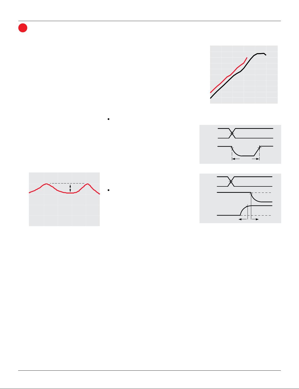
supply voltage. Figure 2 is an example
of r
ON(flat)
.
Typical r
ON(flat)
Measurement
On/Off Capacitance (C
ON
/C
OFF
) —
Total switch and load capacitance
must be considered because it can
affect response time, settling time and
fanout limits.
'SFRVFODZ3FTQPOTF — All CMOS
switches have an upper limit to the
GSFRVFODZUIBUDBOCFQBTTFE/P
matter how low r
ON
and C
I/O
can be
maintained in the chip manufacturing
process, they still form an undesired
low-pass filter that attenuates the
switch output signal.
Sine-Wave Distortion or Total Harmonic
Distortion (THD) — These are measure-
ments of the linearity of the device.
Nonlinearity can be introduced in a
number of ways (design, device
physics, etc.); but typically the largest
contributor is r
ON
, which varies with
V
I/O
for all types of CMOS switches.
Having a low r
ON
is important, but
a flat r
ON
over the signal range is as
FRVBMMZJNQPSUBOU'PSTJHOBMSBOHFTPG
0 < V
I/O
< (V
– 2 V), n-channel switch-
es exhibit very flat r
ON
characteristics;
but r
ON
increases very rapidly as V
I/O
approaches V
and VGS decreases.
Parallel n-/p-channel switches offer
good r
ON
flatness for signal ranges of
0 < V
I/O
< V
, with the best flatness
characteristic at the highest recom-
mended switch V
.
Crosstalk — There are two types of
crosstalk to consider:
r $POUSPMFOBCMFUPPVUQVU5IF
level of crosstalk is a mea sure of how
well decoupled the switch control
signal is from the switch output. Due
to the parasitic capacitance of CMOS
processes, changing the state on the
control signal causes noise to appear
on the output. In audio applications,
this can be a source of the annoying
pop that is sometimes heard when
switching the unit on or off.
r#FUXFFOTXJUDIFT5IFMFWFM
of crosstalk also is a measure of
adjacent-channel rejection. As with
control-to-output crosstalk, parasitic
capacitance can couple the signal on
one switch with that on another switch.
OFF Isolation — A measurement of
OFF-state switch impedance. It is
NFBTVSFEJOE#BUBTQFDJGJDGSFRVFODZ
with the corresponding channel (NC to
COM or NO to COM) in the OFF state.
Feedthrough — This characteristic
is related to the ability of the switch
to block signals when off. As with
crosstalk, parasitic capacitance allows
IJHIGSFRVFODJFTUPDPVQMFUISPVHIUIF
switch, making it appear to be on.
Charge Injection (Q) — TI specifies
enable-to-output crosstalk, and some
competitors use this parameter. As
with enable-to-output crosstalk,
changing the state on the control pin
causes a charge to be coupled to the
channel of the transistor, introducing
signal noise. It is presented in this
report for a relative comparison
with the competition. A graph of
bias voltage vs. charge injection is
displayed in figure 3 above.
Typical Charge Injection Plot
Typical BBM Timing
Typical MMB Timing
t
BBM
50%
90% 90%
Logic
Input
(V
I
)
Switch
Output
(V
COM
)
V
+
0
50%
Logic
Input
(V
I
)
V
+
0
t
MBB
0.8 V
OUT
0.8 V
V
NC
Switch
Output
V
NO
OUT
Break-Before-Make (BBM) Time —
Guarantees that two multiplexer paths
are never electrically connected when
the signal path is changed by the
select input. This parameter is
measured under a specified range
of conditions and by the propagation
delay between the output of two ad-
jacent analog channels (NC and NO),
when the control signal changes state
(as shown in figure 4 above).
Make-Before-Break (MBB) Time —
Guarantees that two multiplexer paths
are never open when the signal path
is changed by the select input. This
parameter is measured under a
specified range of conditions and
by the propagation delay between
the output of two adjacent analog
channels (NC and NO), when the
control signal changes state (as shown
in figure 5 above).
Fig. 2
Fig. 3
Fig. 4
Fig. 5


 我的内容管理
展开
 我的资源
快来上传第一个资源
 我的收益 登录查看自己的收益
 我的积分
登录查看自己的积分
 我的C币
登录后查看C币余额
 我的收藏
我的收藏  我的下载
我的下载  下载帮助
下载帮助 
 前往需求广场,查看用户热搜

 信息提交成功