3PEAK运放TP09-SR 中文手册
需积分: 34 129 浏览量
2022-10-22
19:40:35
上传
评论
收藏 844KB PDF 举报

1
TP09
Stable 6MHz, Low Cost Dual Op Amp
www.3peakic.com Rev. A
Features
Stable 6 MHz GBWP in V
CM
from 0-V to V
DD
Excellent EMI Suppress Performance
Offset Voltage: ±400 μV Maximum
Offset Voltage Temperature Drift: 1 μV/°C
Input Bias Current: 1 pA Typical
THD+Noise: -115 dB at 1kHz, -99 dB at 10kHz
High CMRR/PSRR: 110/95 dB
Beyond the Rails Input Common-Mode Range
Outputs Swing to within 3 mV of Each Rail
No Phase Reversal for Overdriven Inputs
High Output Capability: 100mA
Supply Voltage Range:
- Single +2.1 V to +6.0 V Supply
- Or Dual ±1.05 V to ±3.0 V Supplies
–40°C to 125°C Operation Temperature Range
ESD Rating: 8KV – HBM, 2KV–CDM and 500V–MM
Green, Popular Type Package
Applications
Multimedia Audio
Headphone Drivers
LCD Drivers
Photo Diode Pre-amp
Medical Equipments
Portable Devices
ASIC Input or Output
Sensor Interfaces
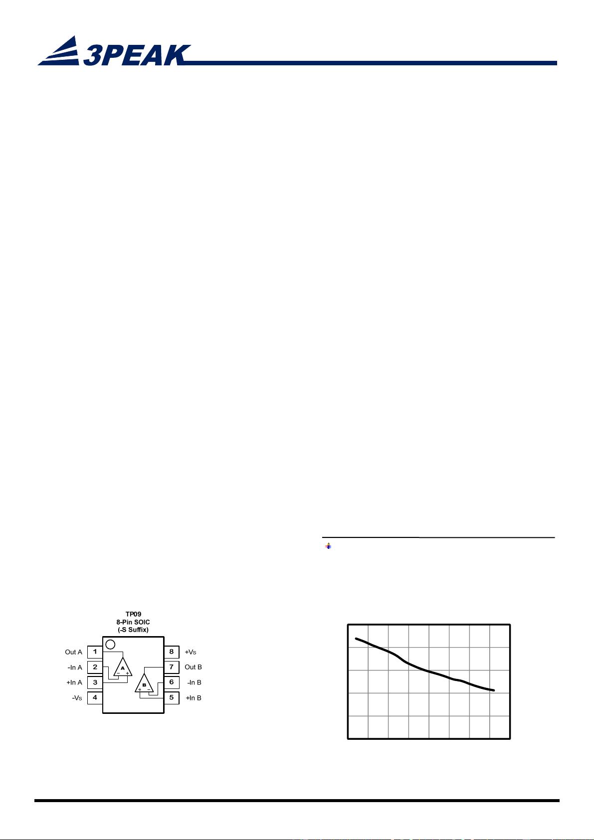
Pin Configuration
(Top View)
Description
The TP09 is CMOS dual RRIO op-amp with low
offset, low power and stable high frequency
response. They incorporate 3PEAK’s proprietary
and patented design techniques to achieve very
good AC performance with 6MHz bandwidth,
4.5V/μs slew rate and low distortion while drawing
only 500μA of quiescent current per amplifier. The
input common-mode voltage range extends 300mV
beyond V– and V+, and the outputs swing rail-to-rail.
The TP09 can be used as plug-in replacements for
many commercially available op-amps to reduce
power and improve input/output range and
performance.
The TP09 Op-amp is unity gain stable with any
capacitive load. They
operate from either single
+2.1V to +6.0V supply or dual ±1.05V to ±3.0V
supplies. Analog trim and calibration routine reduce
input offset voltage to below 400μV, and proprietary
precision temperature compensation technique
makes offset voltage temperature drift at 1μV/°C.
Adaptive biasing and dynamic compensation
enables the TP09 to achieve ‘THD +Noise’ for
1kHz/10kHz 2V
PP
signal at -115dB/ -99dB. Beyond
the rails input and rail-to-rail output characteristics
allow the full power-supply voltage to be used for
signal range.
The combination of features makes the TP09 ideal
choices for audio amplification of computers, sound
ports, and other consumer Audio. The TP09
Op-amp is very stable, and it is capable of driving
heavy capacitive loads such as those found in LCDs.
The ability to swing rail-to-rail at the inputs and
outputs enables designers to buffer CMOS DACs,
ASICs, or other wide output swing devices in
single-supply systems.
3PEAK and the 3PEAK logo are registered trademarks of
3PEAK INCORPORATED. All other trademarks are the property
of their respective owners.
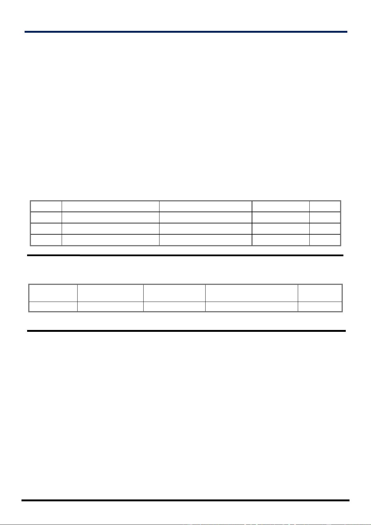
Unity Gain Bandwidth vs. Temperature
0
2
4
6
8
10
‐50 ‐25 0 25 50 75 100 125 150
GBW(MHz)
Temperature(℃)
VCM中从0-V到VDD的稳定6 MHz GBWP
卓越的EMI抑制性能
温度漂移
超出轨道输入共模范围
输出摆幅在每个导轨的3 mV以内
过驱动输入无反相
流行型包装
多媒体音频
耳机驱动程序
光电二极管前置放大器
医疗设备
便携式设备
传感器接口
TP09是CMOS双RRIO运算放大器,具有低失调、低功耗和稳定的高频响应。它们结合了3PEAK的专有和专利设计技术,以实现6MHz带宽、
4.5V/μs转换率和低失真的非常好的交流性能,同时每个放大器仅消耗500μA的静态电流。输入共模电压范围超出V–和V+范围300mV
,输出摆轨至摆轨。TP09可用作许多商用运算放大器的插件替代品,以降低功率并改善输入/输出范围和性能。
TP09运放在任何电容负载下都是单位增益稳定的。它们
在单电源+2.1V至+6.0V或双电源±1.05V至±3.0V下工作
。模拟微调和校准程序将输入偏移电压降至400μV以下
,专有的精密温度补偿技术使偏移电压温度漂移为1μV/
°C。自适应偏置和动态补偿使TP09能够在-115dB/-99dB
的频率下实现1kHz/10kHz 2VPP信号的“THD+噪声”。除
轨道输入和轨道到轨道输出特性外,还允许信号范围使
用全电源电压。
这些功能的结合使TP09成为计算机、声音端口和
其他消费类音频的音频放大的理想选择。TP09运
放非常稳定,能够驱动LCD等重电容负载。在输入
和输出端摆动导轨的能力使设计者能够在单电源
系统中缓冲CMOS DAC、ASIC或其他宽输出摆动设备
。
3PAAK和3PEAK徽标是3PEAKINCORPORATED的注册商标。所有其他商标均为其各自
所有者的财产。
输入偏置电流

剩余12页未读,继续阅读


评论0