LED恒流,6V/20A,最大60V
需积分: 2 10 浏览量
2024-04-01
09:50:11
上传
评论
收藏 1011KB PDF 举报

LT3763
1
Rev. C
For more information www.analog.com
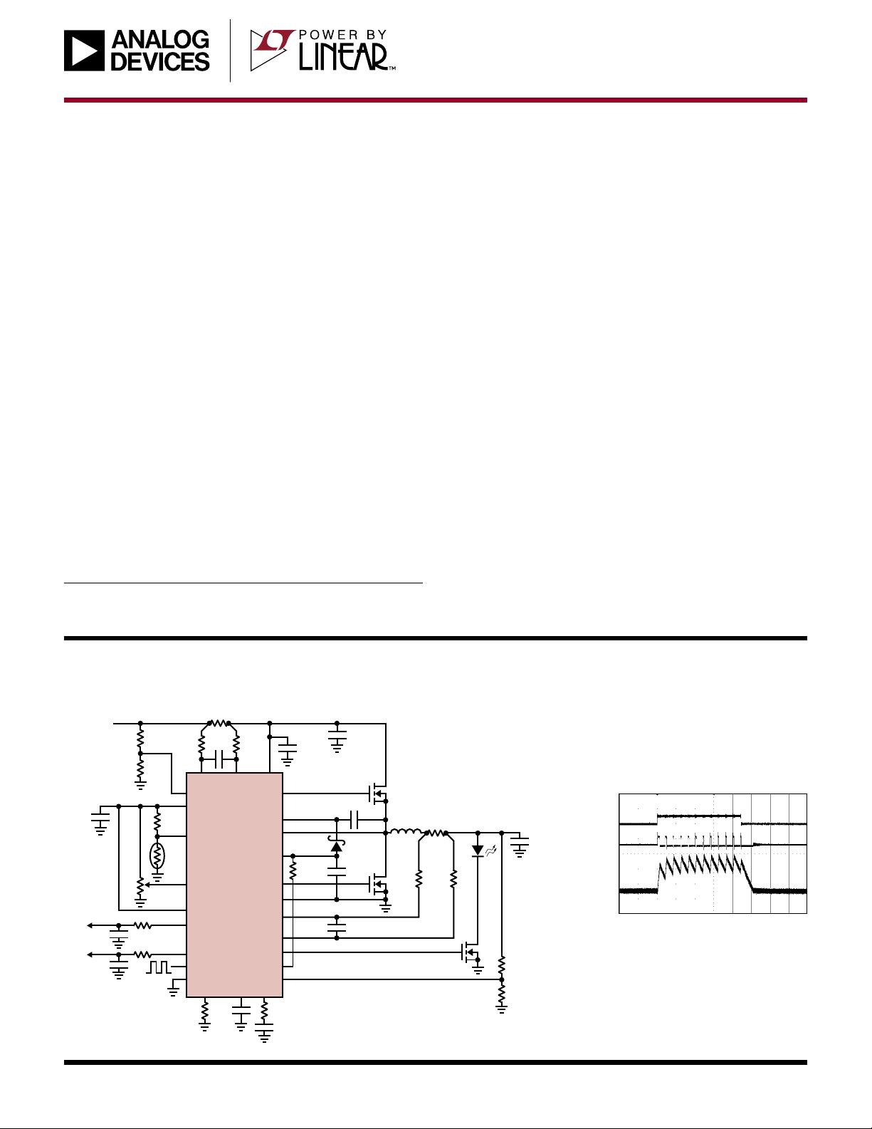
PWM Dimming
PWM
10V/DIV
V
SW
50V/DIV
I
L
5A/DIV
5µs/DIV
3763 TA01b
TYPICAL APPLICATION
FEATURES DESCRIPTION
60V High Current
Step-Down LED Driver Controller
The LT
®
3763 is a fixed frequency, synchronous, step-down
DC/DC controller designed to accurately regulate output
currents up to 20A. The average current mode control
-
ler will maintain inductor current regulation over a wide
output voltage range from 0V to 55V. Output current is
set by analog voltages on the CTRL pins and an external
sense resistor. Voltage regulation and overvoltage protec
-
tion are set with a voltage divider from the output to the
FB
pin. The switching frequency is programmable from
200kHz to 1MHz through an external resistor on the RT
pin or with the SYNC pin and an external clock signal.
Input and output current sensing provides input current
limiting and an accurate measurement of these currents.
The FBIN pin is provided for applications requiring a peak
power tracking function.
Additional features include an accurate external reference
voltage for use with the CTRL pins, an accurate UVLO/
EN pin that allows for programmable UVLO hysteresis,
a PWM driver for LED applications, output voltage fault
detection, and thermal shutdown.
20A, Pulse Width Modulated, Single LED Driver
APPLICATIONS
n
Accurately Control Input and Output Current
n
3000:1 True Color PWM™ Dimming
n
±1.5% Voltage Regulation Accuracy
n
±6% Current Regulation Accuracy
n
6V to 60V Input Voltage Range
n
Wide Output Range Up to 55V
n
<2µA Shutdown Current
n
Control Pin for Thermal Control of Load Current
n
Input and Output Current Monitor and Limit
n
Open, Short, and C/10 Fault Detection
n
PWM Driver Output for LED Applications
n
Thermally Enhanced 28-Lead FE Package
n
High Power Architectural Lighting
n
Automotive Lighting
n
Aviation and Marine Strobe Lights
n
Solar-Powered Chargers, Laser Diodes
100µF
V
IN
10V TO 30V
2.5mΩ
1k 1k
82.5k
EN/UVLO
FBIN
TG
V
IN
BOOST
V
REF
CTRL1
CTRL2
LT3763
SW
BG
GND
V
C
SENSE
+
SENSE
–
INTV
CC
220nF
1.5µH
22µF
2.5mΩ
FB
FAULT
59k
4.7nF
47.5k
3763 TA01
12.1k
2.2µF
470k
PWMOUT
V
OUT
6V, 20A MAXIMUM
220µF
×2
PWM
SYNC
SS
10nF
RT
45.3k
84.5k
15.4k
33nF
10Ω 10Ω
47.5kΩ
1µF
50k
4.7µF
IVINNIVINP
IVINMON
ISMON
1nF
1nF
50Ω
50Ω
All registered trademarks and trademarks are the property of their respective owners.
Document Feedback
剩余29页未读,继续阅读
资源评论


ltqshs
- 粉丝: 6w+
- 资源: 220


最新资源
- ch05-卷积神经网络(CNN).zip
- 操作系统实验二:存储管理(分析XV6分页存储地址变换)
- 一个MATLAB画图的进阶示例,展示如何绘制具有颜色映射的三维表面图,并添加图例和注释
- 前程无忧大数据.xlsx
- JavaMail-jar
- 推荐系统实战练习项目和源码.rar
- 微机原理与接口技术HQFC-A系列USB实验
- 联想笔记本维修图纸:Lenovo V130-15IKB Wistron LV315KB 17807 17807-1 17807
- 一个MATLAB GUI进阶示例,展示如何创建一个简单的用户界面,该界面使用户能够输入两个数值,执行加法运算,并显示结果
- JavaScript 基础学习1(js引入方式、基础使用、核心语法、复合类型) 示例代码
资源上传下载、课程学习等过程中有任何疑问或建议,欢迎提出宝贵意见哦~我们会及时处理!
点击此处反馈


