电压电流转换电流0-20ma电流输出
需积分: 2 146 浏览量
2024-02-08
16:41:14
上传
评论
收藏 1.9MB PDF 举报

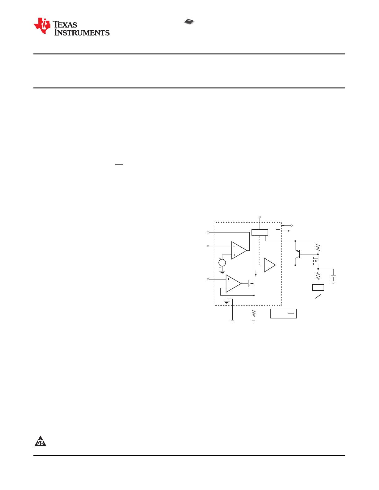
XRT111
3V
REGF
Regulator
Out
Signal
Input
REGS
24V
I-Mirror
VSP
1
9
8
2
VG
IS
OutputDisable
OutputFailure
OD
EF
V
IN
6
4
5
R
SET
I
SET
SET
710
GND
I =10
OUT
()
V
VIN
R
SET
I 10
OUT
SET
= · I
XTR111
Q
2
(1)
Q
1
15W
15W
S
D
G
10nF
0mAto20mA
4mAto20mA
Load
(±LoadGround)
3
XTR111
www.ti.com
SBOS375C –NOVEMBER 2006– REVISED JUNE 2011
Precision Voltage-to-Current
Converter/Transmitter
Check for Samples: XTR111
1
FEATURES
DESCRIPTION
The XTR111 is a precision voltage-to-current
2
• EASY-TO-DESIGN INPUT/OUTPUT RANGES:
converter designed for the standard 0mA–20mA or
0mA–20mA, 4mA–20mA, 5mA–25mA AND
4mA–20mA analog signals, and can source up to
VOLTAGE OUTPUTS
36mA. The ratio between input voltage and output
• NONLINEARITY: 0.002%
current is set by the single resistor R
SET
. The circuit
• LOW OFFSET DRIFT: 1μV/°C
can also be modified for voltage output.
• ACCURACY: 0.015%
An external P-MOSFET transistor ensures high
• SINGLE-SUPPLY OPERATION
output resistance and a broad compliance voltage
• WIDE SUPPLY RANGE: 7V to 44V
range that extends from 2V below the supply voltage,
• OUTPUT ERROR FLAG (EF)
V
VSP
, to voltages well below GND.
• OUTPUT DISABLE (OD)
The adjustable 3V to 15V sub-regulator output
• ADJUSTABLE VOLTAGE REGULATOR:
provides the supply voltage for additional circuitry.
3V to 15V
The XTR111 is available in MSOP and DFN
surface-mount packages.
APPLICATIONS
• UNIVERSAL VOLTAGE-CONTROLLED
CURRENT SOURCE
• CURRENT OR VOLTAGE OUTPUT FOR 3-WIRE
SENSOR SYSTEMS
• PLC OUTPUT PROGRAMMABLE DRIVER
• CURRENT-MODE SENSOR EXCITATION
NOTE: (1) See Application Information,
External Current Limit Circuits for other
options.
1
Please be aware that an important notice concerning availability, standard warranty, and use in critical applications of Texas
Instruments semiconductor products and disclaimers thereto appears at the end of this data sheet.
2All trademarks are the property of their respective owners.
PRODUCTION DATA information is current as of publication date.
Copyright © 2006–2011, Texas Instruments Incorporated
Products conform to specifications per the terms of the Texas
Instruments standard warranty. Production processing does not
necessarily include testing of all parameters.


剩余33页未读,继续阅读
资源评论


ltqshs
- 粉丝: 6w+
- 资源: 219


最新资源
- matlab基于线性准则的考虑风力发电不确定性的分布鲁棒优化机组组合
- 基于C语言+stm32f4的modbus tcp上下位机通信项目+上位机由LabVIEW编写+源码+开发文档+视频教程(高分项目
- 基于Python的Struts2漏洞扫描器设计源码
- HTML+CSS制作的个人博客网页.zip
- 基于htmlde 爱心代码,但HTML网页源码.zip
- 51单片机实现LED流水灯
- 基于Python的obEspoir分布式游戏框架设计源码
- 基于python的机械设计实用计算器,可计算电动机,传动装置,V带轮,齿轮,轴,轴承的几何或者力,运动学参数数值+源码+开发文档
- 基于HTML +JavaScript的元旦倒计时代码.docx
- 【Unity资源免费分享】孩子益智小游戏unity 5x系列Baby Doll House Cleaning
资源上传下载、课程学习等过程中有任何疑问或建议,欢迎提出宝贵意见哦~我们会及时处理!
点击此处反馈


