没有合适的资源?快使用搜索试试~ 我知道了~
OPA2171-英文-datasheet-运放
需积分: 1 0 下载量 7 浏览量
2024-02-05
16:43:04
上传
评论
收藏 1.7MB PDF 举报
温馨提示
![preview](https://dl-preview.csdnimg.cn/88810744/0001-438c7e6d5f5a96ec673cc32d31378fc0_thumbnail.jpeg)
![preview-icon](https://csdnimg.cn/release/downloadcmsfe/public/img/scale.ab9e0183.png)
试读
52页
OPA2171-英文-datasheet-运放
资源推荐
资源详情
资源评论
![zip](https://img-home.csdnimg.cn/images/20210720083646.png)
![zip](https://img-home.csdnimg.cn/images/20210720083736.png)
![ms14](https://img-home.csdnimg.cn/images/20210720083646.png)
![7z](https://img-home.csdnimg.cn/images/20210720083312.png)
![](https://csdnimg.cn/release/download_crawler_static/88810744/bg1.jpg)
1000
800
600
400
200
0
-200
-400
-600
-800
-1000
V (µV)
OS
-20 -15 -10 -5 0 5 10 15 20
V (V)
CM
V = -18.1 V
CM
10 Typical Units Shown
350
250
150
50
-50
-150
-250
-350
V (µV)
OS
0 2 4 6 8 16 20
V (V)
SUPPLY
V = ±2.25 V to ±18 V
SUPPLY
10 Typical Units Shown
18141210
Product
Folder
Order
Now
Technical
Documents
Tools &
Software
Support &
Community
Reference
Design
An IMPORTANT NOTICE at the end of this data sheet addresses availability, warranty, changes, use in safety-critical applications,
intellectual property matters and other important disclaimers. PRODUCTION DATA.
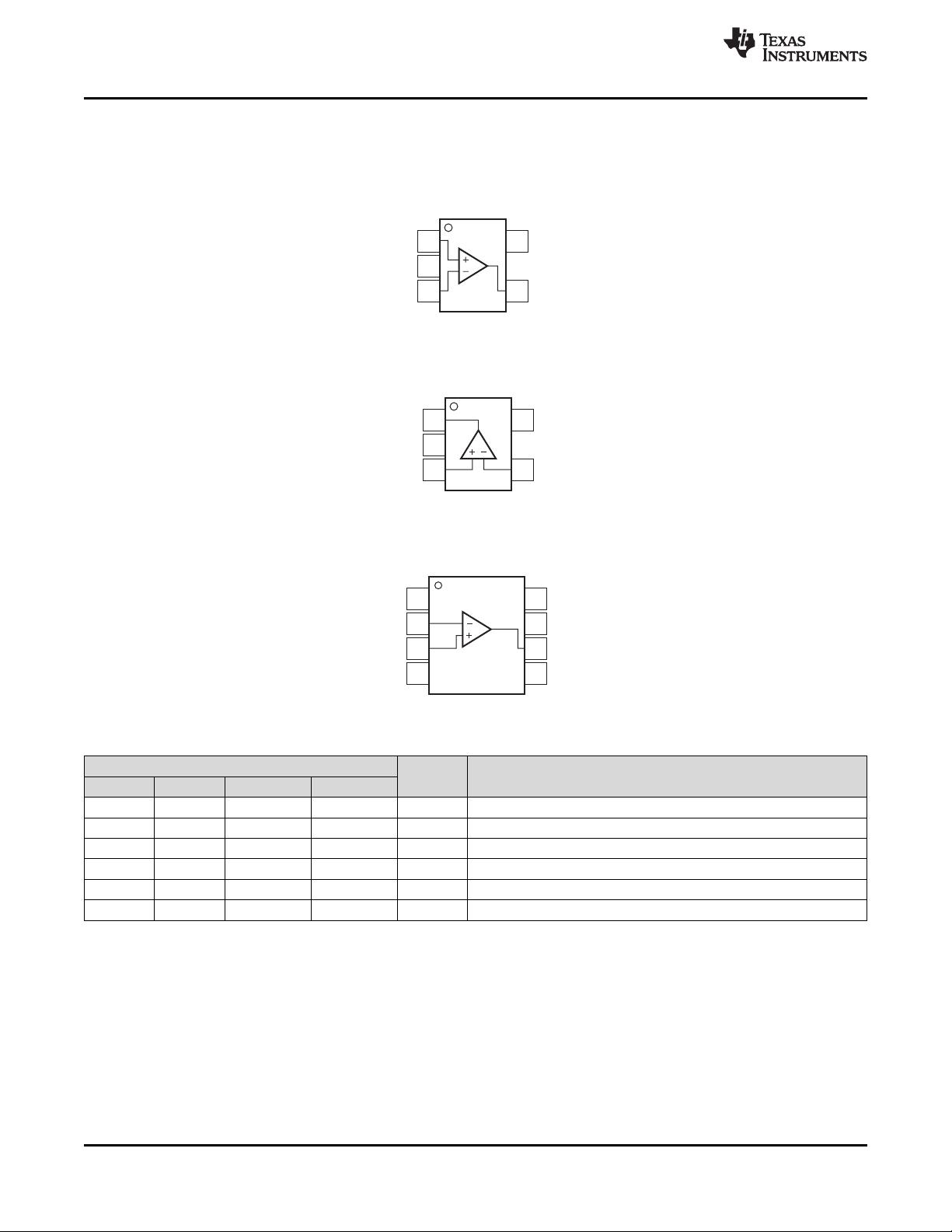
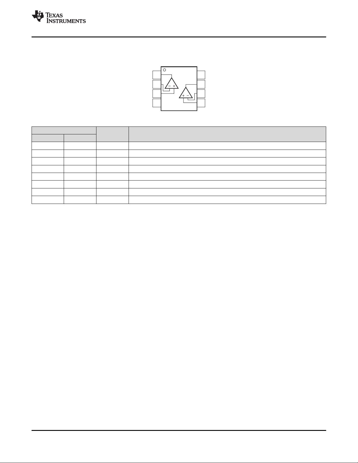
OPA171
,
OPA2171
,
OPA4171
SBOS516G –SEPTEMBER 2010–REVISED MAY 2020
OPAx171 36-V, Single-Supply, SOT-553, General-Purpose Operational Amplifiers
1
1 Features
1
• Supply range: 2.7 to 36 V, ±1.35 V to ±18 V
• Low noise: 14 nV/√Hz
• Low offset drift: ±0.3 µV/°C (typical)
• RFI filtered inputs
• Input range includes the negative supply
• Input range operates to positive supply
• Rail-to-rail output
• Gain bandwidth: 3 MHz
• Low quiescent current: 475 µA per amplifier
• High common-mode rejection: 120 dB (typical)
• Low-input bias current: 8 pA
• Industry-standard packages:
– 8-pin SOIC
– 8-pin MSOP
– 14-pin TSSOP
• Micro packages:
– Single in SOT-553
– Dual in VSSOP-8
2 Applications
• Tracking amplifier in power modules
• Merchant power supplies
• Transducer amplifiers
• Bridge amplifiers
• Temperature measurements
• Strain gauge amplifiers
• Precision integrators
• Battery-powered instruments
• Test equipment
SPACE
3 Description
The OPA171, OPA2171, and OPA4171 (OPAx171)
are a family of 36-V, single-supply, low-noise
operational amplifiers with the ability to operate on
supplies ranging from 2.7 V (±1.35 V) to 36 V (±18
V). These devices are available in micro-packages
and offer low offset, drift, and bandwidth with low
quiescent current. The single, dual, and quad
versions all have identical specifications for maximum
design flexibility.
Unlike most operational amplifiers, which are
specified at only one supply voltage, the OPAx171
family is specified from 2.7 to 36 V. Input signals
beyond the supply rails do not cause phase reversal.
The OPAx171 family is stable with capacitive loads
up to 300 pF. The input can operate 100 mV below
the negative rail and within 2 V of the top rail during
normal operation. These devices can operate with full
rail-to-rail input 100 mV beyond the top rail, but with
reduced performance within 2 V of the top rail.
The OPAx171 series of operational amplifiers are
specified from –40°C to +125°C.
Device Information
(1)
PART NUMBER PACKAGE BODY SIZE (NOM)
OPA171 SOT-23 (5) 1.60 mm × 2.90 mm
OPA2171 SOIC (8) 3.90 mm × 4.90 mm
OPA4171
TSSOP (14) 4.40 mm × 5.00 mm
SOIC (14) 3.90 mm × 8.65 mm
(1) For all available packages, see the orderable addendum at
the end of the data sheet.
Offset Voltage vs Common-Mode Voltage Offset Voltage vs Power Supply
![](https://csdnimg.cn/release/download_crawler_static/88810744/bg2.jpg)
2
OPA171
,
OPA2171
,
OPA4171
SBOS516G –SEPTEMBER 2010–REVISED MAY 2020
www.ti.com
Product Folder Links: OPA171 OPA2171 OPA4171
Submit Documentation Feedback Copyright © 2010–2020, Texas Instruments Incorporated
Table of Contents
1 Features.................................................................. 1
2 Applications ........................................................... 1
3 Description ............................................................. 1
4 Revision History..................................................... 2
5 Pin Configuration and Functions......................... 4
6 Specifications......................................................... 7
6.1 Absolute Maximum Ratings ...................................... 7
6.2 ESD Ratings.............................................................. 7
6.3 Recommended Operating Conditions....................... 7
6.4 Thermal Information: OPA171 .................................. 8
6.5 Thermal Information: OPA2171 ................................ 8
6.6 Thermal Information: OPA4171 ................................ 8
6.7 Electrical Characteristics........................................... 9
6.8 Typical Characteristics............................................ 12
7 Detailed Description............................................ 18
7.1 Overview ................................................................. 18
7.2 Functional Block Diagram ....................................... 18
7.3 Feature Description................................................. 18
7.4 Device Functional Modes........................................ 20
8 Application and Implementation ........................ 21
8.1 Application Information............................................ 21
8.2 Typical Application ................................................. 23
9 Power Supply Recommendations...................... 27
10 Layout................................................................... 27
10.1 Layout Guidelines ................................................ 27
10.2 Layout Example .................................................... 27
11 Device and Documentation Support ................. 28
11.1 Related Links ........................................................ 28
11.2 Support Resources ............................................... 28
11.3 Trademarks........................................................... 28
11.4 Electrostatic Discharge Caution............................ 28
11.5 Glossary................................................................ 28
12 Mechanical, Packaging, and Orderable
Information ........................................................... 28
4 Revision History
NOTE: Page numbers for previous revisions may differ from page numbers in the current version.
Changes from Revision F (April 2018) to Revision G Page
• Added links to Applications .................................................................................................................................................... 1
• Changed graphs with incorrect units (mV to µV) in the Typical Characteristics section...................................................... 12
Changes from Revision E (April 2015) to Revision F Page
• Changed minimum supply voltage value from ±20 V to 0 V in Absolute Maximum Ratings table ....................................... 7
• Added maximum supply voltage value of 40 V to Absolute Maximum Ratings table ........................................................... 7
• Rewrote Electrical Overstress subsection content in Application Information section ........................................................ 21
Changes from Revision D (September 2012) to Revision E Page
• Changed device title (removed "Value Line Series").............................................................................................................. 1
• Added ESD Ratings table, Feature Description section, Device Functional Modes, Application and Implementation
section, Power Supply Recommendations section, Layout section, Device and Documentation Support section, and
Mechanical, Packaging, and Orderable Information section ................................................................................................. 1
Changes from Revision C (June 2011) to Revision D Page
• Added "Value Line Series" to title........................................................................................................................................... 1
Changes from Revision B (November 2010) to Revision C Page
• Added MSOP-8 package to device graphic ........................................................................................................................... 1
• Added MSOP-8 package to Features bullets ......................................................................................................................... 1
• Added MSOP-8 package to Product Family table.................................................................................................................. 1
• Updated pinout configurations for OPA2171 and OPA4171 .................................................................................................. 4
• Added MSOP-8 package to OPA2171 Thermal Information table......................................................................................... 8
![](https://csdnimg.cn/release/download_crawler_static/88810744/bg3.jpg)
3
OPA171
,
OPA2171
,
OPA4171
www.ti.com
SBOS516G –SEPTEMBER 2010–REVISED MAY 2020
Product Folder Links: OPA171 OPA2171 OPA4171
Submit Documentation FeedbackCopyright © 2010–2020, Texas Instruments Incorporated
• Added new row for Voltage Output Swing from Rail parameter to Output subsection of Electrical Characteristics............ 10
• Changed Voltage Output Swing from Rail parameter to over temperature in Output subsection of Electrical
Characteristics...................................................................................................................................................................... 10
• Changed Figure 9................................................................................................................................................................. 12
Changes from Revision A (November, 2010) to Revision B Page
• Changed input offset voltage specification............................................................................................................................. 9
• Changed input offset voltage, over temperature specification ............................................................................................... 9
• Changed quiescent current per amplifier, over temperature specification ........................................................................... 10
![](https://csdnimg.cn/release/download_crawler_static/88810744/bg4.jpg)
1
2
3
4
8
7
6
5
NC
(1)
V+
OUT
NC
(1)
NC
(1)
-IN
+IN
V-
1
2
3
5
4
V+
-IN
OUT
V-
+IN
1
2
3
5
4
V+
OUT
IN+
V-
IN-
4
OPA171
,
OPA2171
,
OPA4171
SBOS516G –SEPTEMBER 2010 –REVISED MAY 2020
www.ti.com
Product Folder Links: OPA171 OPA2171 OPA4171
Submit Documentation Feedback Copyright © 2010–2020, Texas Instruments Incorporated
5 Pin Configuration and Functions
OPA171 DRL Package
5-Pin SOT-553
Top View
OPA171 DBV Package
5-Pin SOT-23
Top View
OPA171 D Package
8-Pin SOIC
Top View
(1) NC - no internal connection
Pin Functions: OPA171
PIN
I/O DESCRIPTION
NAME DRL DBV D
+IN 1 3 3 I Noninverting input
–IN 3 4 2 I Inverting input
OUT 4 1 6 O Output
V+ 5 5 7 — Positive (highest) supply
V– 2 2 4 — Negative (lowest) supply
NC — — 1, 5, 8 — No internal connection (can be left floating)
![](https://csdnimg.cn/release/download_crawler_static/88810744/bg5.jpg)
1
2
3
4
8
7
6
5
V+
OUTB
-INB
+INB
OUTA
-INA
+INA
V-
5
OPA171
,
OPA2171
,
OPA4171
www.ti.com
SBOS516G –SEPTEMBER 2010–REVISED MAY 2020
Product Folder Links: OPA171 OPA2171 OPA4171
Submit Documentation FeedbackCopyright © 2010–2020, Texas Instruments Incorporated
OPA2171 D, DCU, and DCK Packages
8-Pin SO, VSSOP and MSOP
Top View
Pin Functions: OPA2171
PIN
I/O DESCRIPTION
NAME NO.
+IN A 3 I Noninverting input
+IN B 5 I Noninverting input
–IN A 2 I Inverting input
–IN B 6 O Inverting input
OUT A 1 O Output
OUT B 7 — Output
V+ 8 — Positive (highest) supply
V– 4 — Negative (lowest) supply
剩余51页未读,继续阅读
资源评论
![avatar-default](https://csdnimg.cn/release/downloadcmsfe/public/img/lazyLogo2.1882d7f4.png)
![avatar](https://profile-avatar.csdnimg.cn/default.jpg!1)
ltqshs
- 粉丝: 6w+
- 资源: 220
上传资源 快速赚钱
我的内容管理 展开
我的资源 快来上传第一个资源
我的收益
登录查看自己的收益我的积分 登录查看自己的积分
我的C币 登录后查看C币余额
我的收藏
我的下载
下载帮助
![voice](https://csdnimg.cn/release/downloadcmsfe/public/img/voice.245cc511.png)
![center-task](https://csdnimg.cn/release/downloadcmsfe/public/img/center-task.c2eda91a.png)
安全验证
文档复制为VIP权益,开通VIP直接复制
![dialog-icon](https://csdnimg.cn/release/downloadcmsfe/public/img/green-success.6a4acb44.png)