没有合适的资源?快使用搜索试试~ 我知道了~
tps5432-补偿回路
1.该资源内容由用户上传,如若侵权请联系客服进行举报
2.虚拟产品一经售出概不退款(资源遇到问题,请及时私信上传者)
版权申诉
0 下载量 124 浏览量
2022-05-23
17:44:05
上传
评论
收藏 2.29MB PDF 举报
温馨提示
试读
33页
tps5432-补偿回路
资源推荐
资源详情
资源评论
PH
VIN
BOOT
VSENSE
COMP
TPS5432
EN
SS
INPUT
3-6 V
GND
Cin
10 F
10 V
m
Rc
4.99 kW
Cc
3.3 nF
Css
0.01 Fm
2
7
6
8
1
C
BOOT
0.1 F
10 V
m
L
3.3 H
O
m
C
22 Fx2
O
m
1.2 V@3 A
R1
10 kW
R2
20 kW
Cff
390 pF
3
5
4
100
95
90
85
80
75
70
65
60
55
50
Efficiency - %
0 500 1000 1500 2000 2500 3000
Load Current - mA
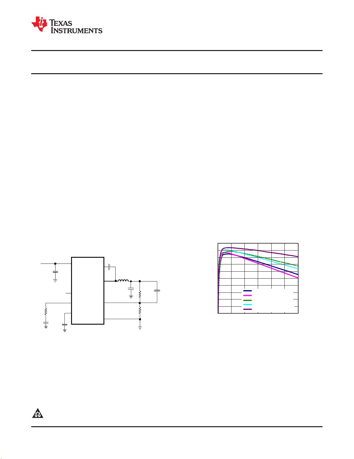
Vin = 5 V, Vout = 1.2 V
Vin = 3.3 V, Vout = 1.2 V
Vin = 5 V, Vout = 1.8 V
Vin = 3.3 V, Vout = 1.8 V
Vin = 5 V, Vout = 3.3 V
TPS5432
www.ti.com.cn
ZHCS854A –MARCH 2012–REVISED OCTOBER 2012
2.95V 至至 6V 输输入入电电压压,,3A 输输出出电电流流,,700kHz 同同步步降降压压转转换换器器
查查询询样样品品: TPS5432
1
特特性性
说说明明
2
• 两两个个用用于于生生成成 3A 持持续续输输出出电电流流的的 70mΩ((典典型型
TPS5432 是一款带有集成型 MOSFET 的 6V,3A,低
值值))场场效效应应管管 (MOSFET)
静态电流 (Iq),电流模式,同步单片降压转换器。
• 带带有有外外部部补补偿偿的的电电流流模模式式控控制制
TPS5432 通过集成 MOSFET、执行电流模式控制来实
• 700kHz 开开关关频频率率
现小型设计,从而减少外部组件数量、使用 700kHz 开
• 360µA 无无负负载载静静态态工工作作电电流流((没没有有开开关关))
关频率来减小电感器尺寸。 带有外露散热垫的 SOIC-8
• 内内部部电电压压基基准准为为 0.808V
封装方式提供耐热增强型解决方案并且易于使用。
• 25°C 时时,,基基准准精精度度为为 ±2.0%
TPS5432 在温度范围内提供带有精确电压基准 (3.0%)
• -40°C~125°C 温温度度范范围围内内 ±3.0% 的的基基准准精精度度
的针对多种负载的准确调节。
• 与与陶陶瓷瓷输输出出电电容容器器一一起起工工作作时时保保持持稳稳定定运运行行
通过集成的 70mΩ MOSFET 和典型值为 360μA 的电
• 可可调调节节慢慢启启动动
源电流,效率得以大幅提升。 通过使用使能引脚进入
• 逐逐周周期期电电流流限限制制、、和和频频率率折折返返保保护护功功能能
关断模式,关断电流可减少至 2µA。
• 耐耐热热增增强强型型 8 引引脚脚小小外外形形尺尺寸寸集集成成电电路路 (SOIC)
(DDA) 封封装装
输出电压启动斜坡由慢启动引脚控制。 一个位于此引
脚上的陶瓷电容器可以很容易的调节慢启动时间。
应应用用范范围围
频率折返和热关断功能在过流情况下保护器件不受损
• 诸诸如如数数字字电电视视 (DTV)、、机机顶顶盒盒、、LCD 显显示示器器、、用用户户
端端设设备备 (CPE) 的的消消费费类类应应用用 坏。
• 针针对对片片上上系系统统 (SoC),,CPU,,数数字字信信号号处处理理器器
(DSP) 的的低低压压负负载载点点调调节节
简简化化的的原原理理图图
1
Please be aware that an important notice concerning availability, standard warranty, and use in critical applications of
Texas Instruments semiconductor products and disclaimers thereto appears at the end of this data sheet.
2PowerPAD is a trademark of Texas Instruments.
PRODUCTION DATA information is current as of publication date.
Copyright © 2012, Texas Instruments Incorporated
Products conform to specifications per the terms of the Texas
Instruments standard warranty. Production processing does not English Data Sheet: SLVSB89
necessarily include testing of all parameters.
1
2
3
4
8
7
6
5
BOOT
VIN
PH
GND
SS
EN
COMP
VSENSE
Thermal
Pad
TPS5432
ZHCS854A –MARCH 2012–REVISED OCTOBER 2012
www.ti.com.cn
These devices have limited built-in ESD protection. The leads should be shorted together or the device placed in conductive foam
during storage or handling to prevent electrostatic damage to the MOS gates.
PIN CONFIGURATION
SO-8 WITH THERMAL PAD
(TOP VIEW)
PIN FUNCTIONS
PIN
DESCRIPTION
NAME NUMBER
A bootstrap cap is required between BOOT and PH. If the voltage on this cap is below the minimum
BOOT 1
required by the output device, the output is forced to switch off until the cap is refreshed.
Error amplifier output, and input to the output switch current comparator. Connect frequency compensation
COMP 6
to this pin.
This pin has an internal pull up which enables switching if left open. To disable switching and reduce
EN 7
quiescent current, this pin must be pulled to ground.
GND 4 Ground. This pin should be electrically connected directly to the thermal pad under the IC
The source of the internal high side power MOSFET, and drain of the internal low side (synchronous)
PH 3
rectifier MOSFET.
SS 8 Slow start time setting. An external capacitor connected to this pin sets the output rise time
GND pin should be connected to the exposed thermal pad for proper operation. This thermal pad should
THERMAL PAD 9
be connected to any internal PCB ground plane using multiple vias for good thermal performance.
VIN 2 Supplies the control circuitry and switches of the power converter. The range is 2.95V to 6V.
VSENSE 5 Inverting node of the gm error amplifier.
ORDERING INFORMATION
(1)
T
j
PACKAGE
(2) (3)
ORDERABLE PART NUMBER
Tube TPS5432DDA
–40°C to 125°C 8-pin SOIC PowerPAD™
Tape and Reel TPS5432DDAR
(1) For the most current package and ordering information, see the Package Option Addendum at the end of this document, or see the TI
web site at www.ti.com.
(2) Package drawings, thermal data, and symbolization are available at www.ti.com/packaging.
(3) All package options have Cu NIPDAU lead/ball finish.
2 Copyright © 2012, Texas Instruments Incorporated
TPS5432
www.ti.com.cn
ZHCS854A –MARCH 2012–REVISED OCTOBER 2012
ABSOLUTE MAXIMUM RATING
(1)
VALUE
UNIT
MIN MAX
VIN –0.3 7
EN –0.3 3.6
BOOT PH + 7
Input voltage V
VSENSE –0.3 3
COMP –0.3 3
SS –0.3 3
BOOT-PH 7
Output voltage PH –0.6 7 V
PH 10 ns Transient –2 10
Source current EN 100 µA
COMP 100
Sink current µA
SS 100
Electrostatic discharge (HBM) QSS 009-105 (JESD22-A114A)
(2)
2 kV
Electrostatic discharge (CDM) QSS 009-147 (JESD22-C101B.01) 500 V
T
J
–40 150
Temperature °C
T
stg
–65 150
(1) Stresses beyond those listed under absolute maximum ratings may cause permanent damage to the device. These are stress ratings
only, and functional operation of the device at these or any other conditions beyond those indicated under ELECTRICAL
SPECIFICATIONS is not implied. Exposure to absolute-maximum-rated conditions for extended periods may affect device reliability.
(2) The human body model is a 100-pF capacitor discharge through a 1.5-kΩ resistor into each pin. The machine model is a 200-pF
capacitor discharged directly into each pin.
THERMAL INFORMATION
TPS5432
THERMAL METRIC
(1)
UNITS
DDA (8 PINS)
θ
JA
Junction-to-ambient thermal resistance 42.1
θ
JCtop
Junction-to-case (top) thermal resistance 50.9
θ
JB
Junction-to-board thermal resistance 31.8
°C/W
ψ
JT
Junction-to-top characterization parameter 5
ψ
JB
Junction-to-board characterization parameter 13.5
θ
JCbot
Junction-to-case (bottom) thermal resistance 7.1
spacer
(1) 有关传统和新的热 度量的更多信息,请参阅IC
封装热度量
应用报告, SPRA953。
spacer
Copyright © 2012, Texas Instruments Incorporated 3
TPS5432
ZHCS854A –MARCH 2012–REVISED OCTOBER 2012
www.ti.com.cn
ELECTRICAL CHARACTERISTICS
The Electrical Ratings specified in this section apply to all specifications in this document, unless otherwise noted. These
specifications are interpreted as conditions that do not degrade the parametric or functional specifications of the device for the
life of the product containing it. Test Conditions: T
J
= –40°C to 125°C, VIN = 2.95 to 6V, (unless otherwise noted)
PARAMETERS CONDITIONS MIN TYP MAX UNIT
SUPPLY VOLTAGE
Vin 2.95 6 V
Iq shutdown EN = 0V, 25°C, 2.95 V < Vin < 6 V 2 5 µA
Iq operating No load, Vin = 5 V, no switching, Vsense = 1 V, 25°C 360 575 µA
VIN UVLO
Input UVLO threshold Rising Vin 2.6 2.8 V
Input UVLO hysteresis 0.2 V
ENABLE
Enable threshold Rising 0.984 1.23 1.47 V
Enable threshold Falling 0.952 1.19
Enable threshold +50 mv –4.6
Input current µA
Enable threshold –50 mv –1.2
VOLTAGE REFERENCE
2.95 V < Vin < 6 V, T
J
= 25°C 0.792 0.808 0.824 V
Reference
2.95 V < Vin < 6 V, –40°C < T
J
< +125°C 0.784 0.808 0.832 V
MOSFET
H.S switch resistance BOOT-PH = 5 V, T
J
= 25°C 62 86 mΩ
L.S switch resistance Vin = 5 V, T
J
= 25°C 73 103 mΩ
H.S switch resistance BOOT-PH = 2.95 V, T
J
= 25°C 88 114 mΩ
L.S switch resistance Vin = 2.95 V, T
J
= 25°C 94 128 mΩ
ERROR AMPLIFIER
Error amp transconductance (gm) –2 µA < ICOMP < 2 µA, V(COMP) = 1 V 245 µmho
Error amp transconductance (gm) during soft start –2 µA < ICOMP < 2 µA,V(COMP) = 1 V, Vsense = 0.3 V 70 µmho
Error amp source/sink V(COMP) = 1 V, 100 mV overdrive ±20 µA
COMP to Iph gm Vin = 5 V, Iph1 = (0.5 or 1A) and Iph2 = 3 A 15 A/V
FREQUENCY FOLDBACK vs. VSENSE
Vsense voltage for Fs foldback 50% frequency 0.4 V
Vsense voltage for Fs foldback 25% frequency 0.2 V
CURRENT LIMIT
I max High side FET Vin = 3.3 V, duty cycle = 100% 3.8 5.7 7 A
I max Low side FET 0.8 1.8 A
THERMAL SHUTDOWN
Thermal Shutdown 155 170 C
OT Hysteresis 15 C
SWITCHING FREQUENCY
Switching frequency 520 700 880 kHz
PH (PH PIN)
Minimum on time Vin = 5 V; Measured at 50% points on PH, Iout = 3 A 120 150 ns
Minimum off time Prior to skipping off pulses, BOOT-PH = 2.95 V, Iout = 3 A 60 ns
Rise/Fall time Vin = 5 V, Io = 0 A 1.5 V/ns
Rise/Fall time Vin = 5 V, Io = 3 A 1.5 V/ns
BOOT
Boot recharge FET resistance Vin = 5 V 15 Ω
Boot UVLO Vin = 2.95 V 2.1 V
SLOW START TIME
Charge current Vss = 0.4 V 2 μA
4 Copyright © 2012, Texas Instruments Incorporated
-50 -25 0 25 50 75 100 125 150
T - Junction Temperature - °C
J
0.780
0.800
0.820
0.840
Vref - Voltage Reference - V
V = 3.3 V
I
-50 -25 0 25 50 75 100 125 150
T - Junction Temperature - °C
J
3
4
5
6
7
8
IcI - High Side Current Limit Threshold - A
V = 3.3 V
I
V = 5 V
I
-50 -25 0 25 50 75 100 125 150
T - Junction Temperature - °C
J
40
50
60
70
80
90
100
110
120
130
Rdson - Static Drain-Source On Resistance - mW
HSF, V = 3.3 V
I
HSF, V = 5 V
I
LSF, V = 3.3 V
I
LSF, V = 5 V
I
650
670
690
710
730
750
f - Switching Frequency - kHz
sw
V =5 V
I
-50 -25 0 25 50 75 100 125 150
T - Junction Temperature - °C
J
TPS5432
www.ti.com.cn
ZHCS854A –MARCH 2012–REVISED OCTOBER 2012
TYPICAL CHARACTERISTICS CURVES
HIGH SIDE & LOW SIDE Rdson FREQUENCY
vs vs
JUNCTION TEMPERATURE JUNCTION TEMPERATURE
Figure 1. Figure 2.
HIGH SIDE CURRENT LIMIT THRESHOLD VOLTAGE REFERENCE
vs vs
JUNCTION TEMPERATURE JUNCTION TEMPERATURE
Figure 3. Figure 4.
Copyright © 2012, Texas Instruments Incorporated 5
剩余32页未读,继续阅读
资源评论
ltqshs
- 粉丝: 6w+
- 资源: 219
上传资源 快速赚钱
- 我的内容管理 展开
- 我的资源 快来上传第一个资源
- 我的收益 登录查看自己的收益
- 我的积分 登录查看自己的积分
- 我的C币 登录后查看C币余额
- 我的收藏
- 我的下载
- 下载帮助
安全验证
文档复制为VIP权益,开通VIP直接复制
信息提交成功