Basic Calculation of an Inverting Buck-Boost Power Stage (Rev. A
版权申诉
32 浏览量
2022-05-23
17:24:25
上传
评论
收藏 431KB PDF 举报

C
I
C
O
V
O
V
I
L
1
D
1
S
1
D
f
(sw)
1-D
f
(sw)
R
O
I
O
1
SLVA721A–February 2017–Revised August 2017
Submit Documentation Feedback
Copyright © 2017, Texas Instruments Incorporated
Basic Calculation of an Inverting Buck-Boost Power Stage
Application Report
SLVA721A–February 2017–Revised August 2017
Basic Calculation of an Inverting Buck-Boost Power Stage
IlonaWeiss
ABSTRACT
This application note provides basic formulas that you need to design the power stage of an inverting
buck-boost converter. The premise is that the power switch is integrated in the IC and the rectification is
done by a diode (non-synchronous power stage). It provides all the formulas and considerations that you
need to select the external power components such as the inductor, the diode, and the input and output
capacitors. As the internal switch current capability is limited it will also provide an estimation to judge
whether the load current can meet the IC specification.
Preconditions for the design:
• Basic understanding of the functionality, refer to this TI Training
• Continous-Conduction-Mode (CCM) consideration
• Large signal consideration
• Integrated switch
• Non-synchronous converter
• Basic understanding of the DC Bias Effect of Ceramic Capacitors
Trademarks
All trademarks are the property of their respective owners.
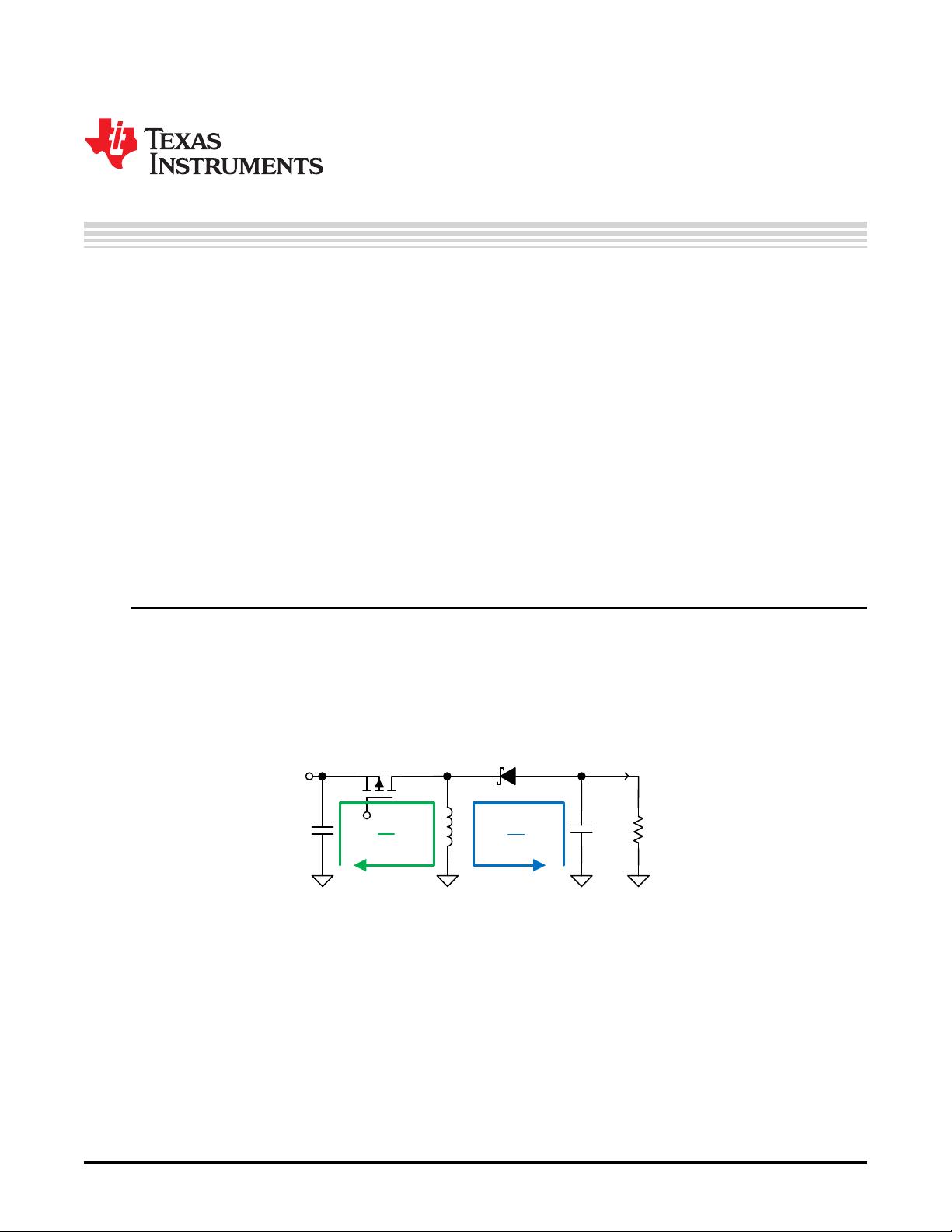
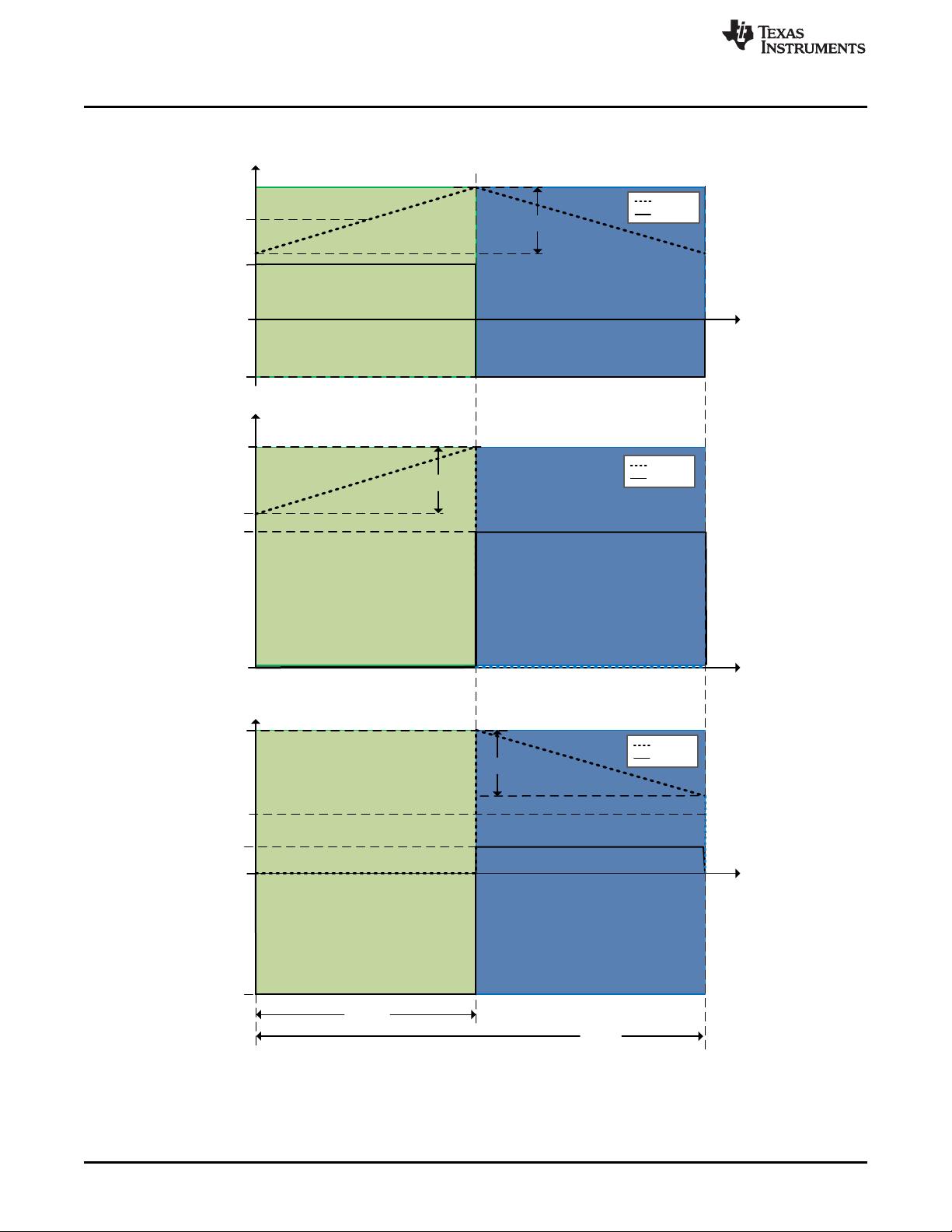
1 Basic Configuration of the Power Stage
Figure 1 shows the simplified schematic of an inverting buck-boost power stage. This topology is a so-
called flyback topology where the energy is transferred to the output when switch S1 is open.
Figure 1. Simplified Schematic of an Inverting Buck-Boost Stage

剩余10页未读,继续阅读


评论0
最新资源