没有合适的资源?快使用搜索试试~ 我知道了~
DDS波形发生器芯片AD9833芯片资料
资源详情
资源评论
资源推荐
Low Power, 12.65 mW, 2.3 V to 5.5 V,
Programmable Waveform Generator
Data Sheet
AD9833
Rev. G Document Feedback
Information furnished by Analog Devices is believed to be accurate and reliable. However, no
responsibility is assumed by Analog Devices for its use, nor for any infringements of patents or other
rights of third parties that may result from its use. Specifications subject to change without notice. No
license is granted by implication or otherwise under any patent or patent rights of Analog Devices.
Trademarks and registered trademarks are the property of their respective owners.
One Technology Way, P.O. Box 9106, Norwood, MA 02062-9106, U.S.A.
Tel: 781.329.4700 ©2003–2019 Analog Devices, Inc. All rights reserved.
Technical Support www.analog.com
FEATURES
Digitally programmable frequency and phase
12.65 mW power consumption at 3 V
0 MHz to 12.5 MHz output frequency range
28-bit resolution: 0.1 Hz at 25 MHz reference clock
Sinusoidal, triangular, and square wave outputs
2.3 V to 5.5 V power supply
No external components required
3-wire SPI interface
Extended temperature range: −40°C to +105°C
Power-down option
10-lead MSOP package
AEC-Q100 qualified for automotive applications
APPLICATIONS
Frequency stimulus/waveform generation
Liquid and gas flow measurement
Sensory applications: proximity, motion,
and defect detection
Line loss/attenuation
Test and medical equipment
Sweep/clock generators
Time domain reflectometry (TDR) applications
GENERAL DESCRIPTION
The AD9833 is a low power, programmable waveform
generator capable of producing sine, triangular, and square
wave outputs. Waveform generation is required in various
types of sensing, actuation, and time domain reflectometry
(TDR) applications. The output frequency and phase are
software programmable, allowing easy tuning. No external
components are needed. The frequency registers are 28 bits
wide: with a 25 MHz clock rate, resolution of 0.1 Hz can be
achieved; with a 1 MHz clock rate, the AD9833 can be tuned to
0.004 Hz resolution.
The AD9833 is written to via a 3-wire serial interface. This serial
interface operates at clock rates up to 40 MHz and is
compatible with DSP and microcontroller standards. The
device operates with a power supply from 2.3 V to 5.5 V.
The AD9833 has a power-down function (SLEEP). This function
allows sections of the device that are not being used to be powered
down, thus minimizing the current consumption of the part. For
example, the DAC can be powered down when a clock output
is being generated.
The AD9833 is available in a 10-lead MSOP package.
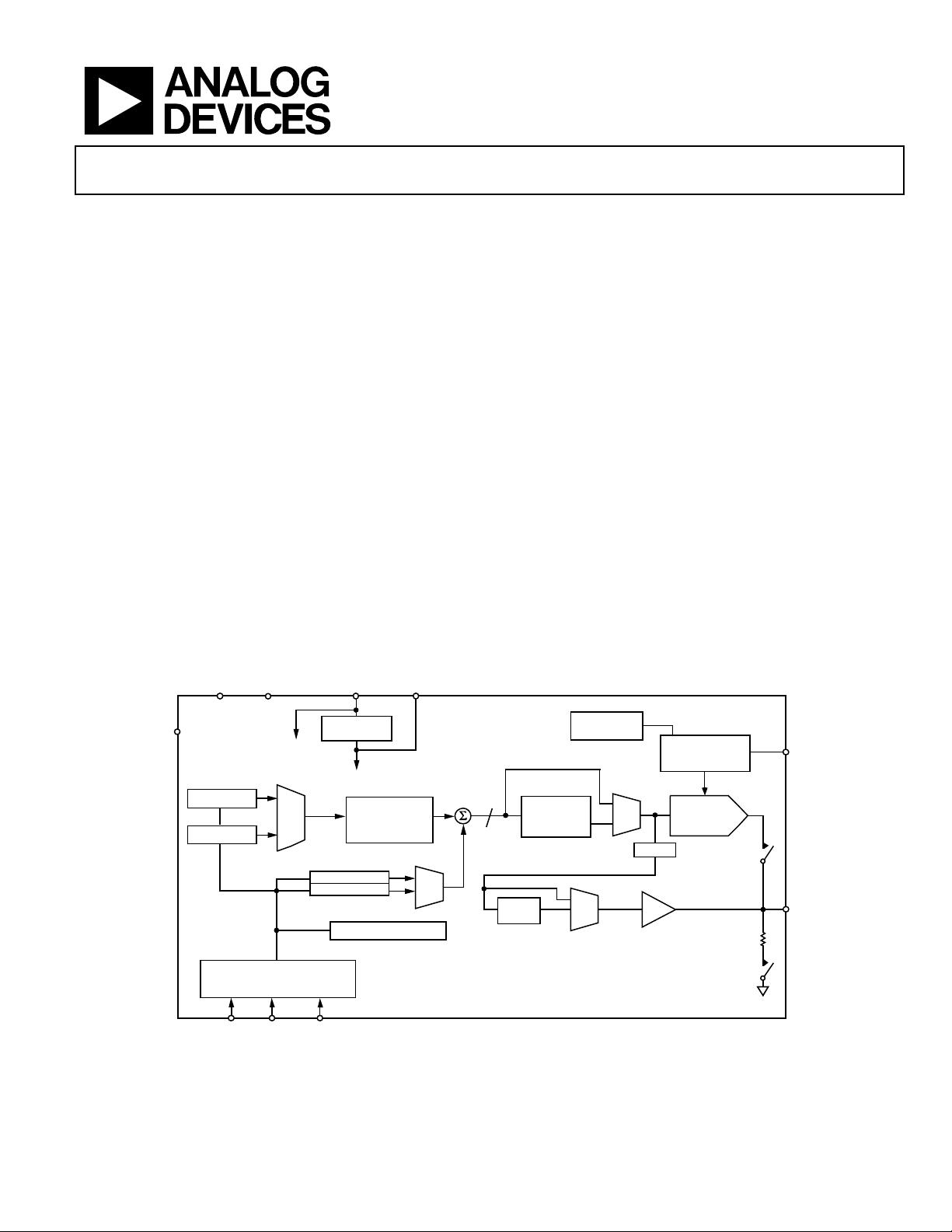
FUNCTIONAL BLOCK DIAGRAM
SERIAL INTERFACE
AND
CONTROL LOGIC
SCLK SDATAFSYNC
CONTROL REGISTER
PHASE1 REG
PHASE0 REG
MUX
SIN
ROM
10-BIT DAC
MUX
FREQ0 REG
FREQ1 REG
12
ON-BOARD
REFERENCE
AGND
DGND
VDD
AD9833
PHASE
ACCUMULATOR
(28-BIT)
REGULATOR
CAP/2.5V
2.5V
AVDD/
DVDD
MUX
DIVIDE
BY 2
MSB
MUX
FULL-SCALE
CONTROL
COMP
VOUT
R
200Ω
MCLK
02704-001
Figure 1.
AD9833 Data Sheet
Rev. G | Page 2 of 21
TABLE OF CONTENTS
Features .............................................................................................. 1
Applications ....................................................................................... 1
General Description ......................................................................... 1
Functional Block Diagram .............................................................. 1
Revision History ............................................................................... 2
Specifications ..................................................................................... 3
Timing Characteristics ................................................................ 4
Absolute Maximum Ratings ............................................................ 5
ESD Caution .................................................................................. 5
Pin Configuration and Function Descriptions ............................. 6
Typical Performance Characteristics ............................................. 7
Terminology .................................................................................... 10
Theory of Operation ...................................................................... 11
Circuit Description ......................................................................... 12
Numerically Controlled Oscillator Plus Phase Modulator ... 12
Sin ROM ...................................................................................... 12
Digital-to-Analog Converter (DAC) ....................................... 12
Regulator ...................................................................................... 12
Functional Description .................................................................. 13
Serial Interface ............................................................................ 13
Powering Up the AD9833 ......................................................... 13
Latency Period ............................................................................ 13
Control Register ......................................................................... 13
Frequency and Phase Registers ................................................ 15
Reset Function ............................................................................ 16
Sleep Function ............................................................................ 16
VOUT Pin ................................................................................... 16
Applications Information .............................................................. 17
Grounding and Layout .............................................................. 17
Interfacing to Microprocessors ..................................................... 20
AD9833 to 68HC11/68L11 Interface ....................................... 20
AD9833 to 80C51/80L51 Interface .......................................... 20
AD9833 to DSP56002 Interface ............................................... 20
Outline Dimensions ....................................................................... 21
Ordering Guide .......................................................................... 21
Automotive Products ................................................................. 21
REVISION HISTORY
4/2019—Rev. F to Rev. G
Change to Features Section ............................................................. 1
Changes to Table 1 ............................................................................ 3
Changes to Ordering Guide .......................................................... 21
4/2018—Rev. E to Rev. F
Updated Format .................................................................. Universal
Changes to AD9833 to 68HC11/68L11 Interface Section ........ 20
Deleted Evaluation Board Section and Figure 32 to Figure 37;
Renumbered Sequentially .............................................................. 21
Changes to Ordering Guide .......................................................... 21
9/2012—Rev. D to Rev. E
Changed Input Current, I
INH
/I
INL
from 10 mA to 10 μA .............. 3
4/2011—Rev. C to Rev. D
Change to Figure 13 ......................................................................... 8
Changes to Table 9 .......................................................................... 15
Deleted AD9833 to ADSP-2101/ADSP-2103 Interface
Section .............................................................................................. 20
Changes to Evaluation Board Section .......................................... 21
Added System Demonstration Platform Section, AD9833
to SPORT Interface Section, and Evaluation Kit Section .......... 21
Changes to Crystal Oscillator vs. External Clock Section
and Power Supply Section ............................................................. 21
Added Figure 32 and Figure 33; Renumbered Figures
Sequentially ..................................................................................... 21
Deleted Prototyping Area Section and Figure 33 ....................... 22
Added Evaluation Board Schematics Section, Figure 34,
and Figure 35 ................................................................................... 22
Deleted Table 16 ............................................................................. 23
Added Evaluation Board Layout Section, Figure 36,
Figure 37, and Figure 38 ................................................................ 23
Changes to Ordering Guide .......................................................... 24
9/2010—Rev. B to Rev. C
Changed 20 mW to 12.65 mW in Data Sheet Title
and Features List ................................................................................ 1
Changes to Figure 6 Caption and Figure 7 ..................................... 7
6/2010—Rev. A to Rev. B
Changes to Features Section ............................................................ 1
Changes to Serial Interface Section .............................................. 13
Changes to VOUT Pin Section ..................................................... 16
Changes to Grounding and Layout Section ................................ 17
Updated Outline Dimensions ....................................................... 24
Changes to Ordering Guide .......................................................... 24
Added Automotive Products Section .......................................... 24
6/2003—Rev. 0 to Rev. A
Updated Ordering Guide ................................................................. 4
Data Sheet AD9833
Rev. G | Page 3 of 21
SPECIFICATIONS
VDD = 2.3 V to 5.5 V, AGND = DGND = 0 V, T
A
= T
MIN
to T
MAX
, R
SET
= 6.8 kΩ for VOUT, unless otherwise noted.
Table 1.
Parameter
1
Min Typ Max Unit Test Conditions/Comments
SIGNAL DAC SPECIFICATIONS
Resolution 10 Bits
Update Rate 25 MSPS
VOUT Maximum 0.65 V
VOUT Minimum 38 mV
VOUT Temperature Coefficient 200 ppm/°C
DC Accuracy
Integral Nonlinearity ±1.0 LSB
Differential Nonlinearity ±0.5 LSB
DDS SPECIFICATIONS (SFDR)
Dynamic Specifications
Signal-to-Noise Ratio (SNR) 55 60 dB
AD9833BRMZ, f
MCLK
= 25 MHz, f
OUT
=
f
MCLK
/4096
54 60 dB
AD9833WBRMZ-REEL, f
MCLK
= 25 MHz, f
OUT
= f
MCLK
/4096
Total Harmonic Distortion (THD) −66 −56 dBc
AD9833BRMZ, f
MCLK
= 25 MHz, f
OUT
=
f
MCLK
/4096
−66 −55 dBc
AD9833WBRMZ-REEL, f
MCLK
= 25 MHz, f
OUT
=
f
MCLK
/4096
Spurious-Free Dynamic Range (SFDR)
Wideband (0 to Nyquist) −60 dBc f
MCLK
= 25 MHz, f
OUT
= f
MCLK
/50
Narrow-Band (±200 kHz) −78 dBc f
MCLK
= 25 MHz, f
OUT
= f
MCLK
/50
Clock Feedthrough −60 dBc
Wake-Up Time 1 ms
LOGIC INPUTS
Input High Voltage, V
INH
1.7 V 2.3 V to 2.7 V power supply
2.0 V 2.7 V to 3.6 V power supply
2.8 V 4.5 V to 5.5 V power supply
Input Low Voltage, V
INL
0.5 V 2.3 V to 2.7 V power supply
0.7 V 2.7 V to 3.6 V power supply
0.8 V 4.5 V to 5.5 V power supply
Input Current, I
INH
/I
INL
10 μA
Input Capacitance, C
IN
3 pF
POWER SUPPLIES f
MCLK
= 25 MHz, f
OUT
= f
MCLK
/4096
VDD 2.3 5.5 V
I
DD
4.5 5.5 mA I
DD
code dependent; see Figure 7
Low Power Sleep Mode 0.5 mA DAC powered down, MCLK running
1
Operating temperature range is −40°C to +105°C; typical specifications are at +25°C.
VOUT
COMP
12
AD9833
10-BIT DAC
SIN
ROM
20pF
10nF
VDD
REGULATOR
100nF
CAP/2.5V
02704-002
Figure 2. Test Circuit Used to Test Specifications
AD9833 Data Sheet
Rev. G | Page 4 of 21
TIMING CHARACTERISTICS
VDD = 2.3 V to 5.5 V, AGND = DGND = 0 V, unless otherwise noted.
1
Table 2.
Parameter Limit at T
MIN
to T
MAX
Unit Description
t
1
40 ns min MCLK period
t
2
16 ns min MCLK high duration
t
3
16 ns min MCLK low duration
t
4
25 ns min SCLK period
t
5
10 ns min SCLK high duration
t
6
10 ns min SCLK low duration
t
7
5 ns min FSYNC to SCLK falling edge setup time
t
8
min
10 ns min FSYNC to SCLK hold time
t
8
max
t
4
− 5 ns max
t
9
5 ns min Data setup time
t
10
3 ns min Data hold time
t
11
5 ns min SCLK high to FSYNC falling edge setup time
1
Guaranteed by design, not production tested.
Timing Diagrams
t
2
t
1
MCLK
t
3
02704-003
Figure 3. Master Clock
t
5
t
4
t
6
t
7
t
8
t
10
t
9
41D51DD0D1D2D14
SCLK
FSYNC
SDATA
D15
t
11
02704-004
Figure 4. Serial Timing
剩余20页未读,继续阅读
海里的鱼2022
- 粉丝: 8289
- 资源: 39
上传资源 快速赚钱
- 我的内容管理 展开
- 我的资源 快来上传第一个资源
- 我的收益 登录查看自己的收益
- 我的积分 登录查看自己的积分
- 我的C币 登录后查看C币余额
- 我的收藏
- 我的下载
- 下载帮助
最新资源
- 论文(最终)_20240430235101.pdf
- 基于python编写的Keras深度学习框架开发,利用卷积神经网络CNN,快速识别图片并进行分类
- 最全空间计量实证方法(空间杜宾模型和检验以及结果解释文档).txt
- 5uonly.apk
- 蓝桥杯Python组的历年真题
- 2023-04-06-项目笔记 - 第一百十九阶段 - 4.4.2.117全局变量的作用域-117 -2024.04.30
- 前端开发技术实验报告:内含4四实验&实验报告
- Highlight Plus v20.0.1
- 林周瑜-论文.docx
资源上传下载、课程学习等过程中有任何疑问或建议,欢迎提出宝贵意见哦~我们会及时处理!
点击此处反馈
安全验证
文档复制为VIP权益,开通VIP直接复制
信息提交成功
评论0