没有合适的资源?快使用搜索试试~ 我知道了~
Feature of MB89R118C 1、2K Bytes FRAM (8 Bytes Block, 256Blocks) 2、13.56MHz: ISO/IEC15693,18000-3(Mode1) 3、ASK 10 / 100% Modulation, 1 out of 4 Data Coding 4、Fast Read/Write Commands (Data rate: 52.97kbps 5、Input Capacitance 24 / 96pF 6、Fast Writing: 1.4sec (2K bytes)
资源推荐
资源详情
资源评论

FUJITSU SEMICONDUCTOR
MEMORY SOLUTION DATA SHEET
Copyright 2022 FUJITSU SEMICONDUCTOR MEMORY SOLUTION LIMITED
2022.07
ASSP
FeRAM Embedded High-speed RFID LSI
MB89R118C
DESCRIPTION
The MB89R118C is a vicinity type of RFID LSI device embedded with 2 Kbytes FeRAM, which enables fast
and frequent write operation.
FEATURES
• Memory capacity of 2 Kbytes FeRAM (including 2000 bytes of user area)
• 8-byte/block configuration, 256 blocks
• High-speed data transmission at 26.48 kbps
• Fast command supported (data transmission at 52.97 kbps) (Transponder Reader/Writer)
• Carrier frequency at 13.56 MHz
• Anti-collision function : 30 tags per second
• Read/Write endurance : 10
12
times
• Data retention : 10 years ( 85 C) , 30 years (+70 C)
• 64-bit UID
• FeRAM memory data protection
• Electronic article surveillance (EAS) command
• Transmission protocol based on ISO/IEC 15693, ISO/IEC18000-3 (Mode 1) (*)
* : Refer to “USAGE NOTES”.
DS411-00001-6v0-E

MB89R118C
2 DS411-00001-6v0-E
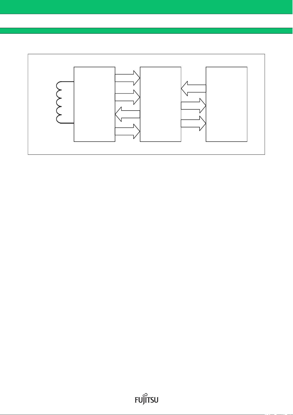
BLOCK DIAGRAM
VDD
R/W
Clock
Data output
Data input
Data output
Data input
Analog RF interface
Digital control
FeRAM
2 Kbytes
Anti-collision
function
I/O
Commands
Rectifier
Clock generator
Power supply
voltage control
Modulator
Antenna
coil
FeRAM access
Demodulator

MB89R118C
DS411-00001-6v0-E 3
MEMORY MAP
This section describes the FeRAM memory, which is the internal memory of the MB89R118C.
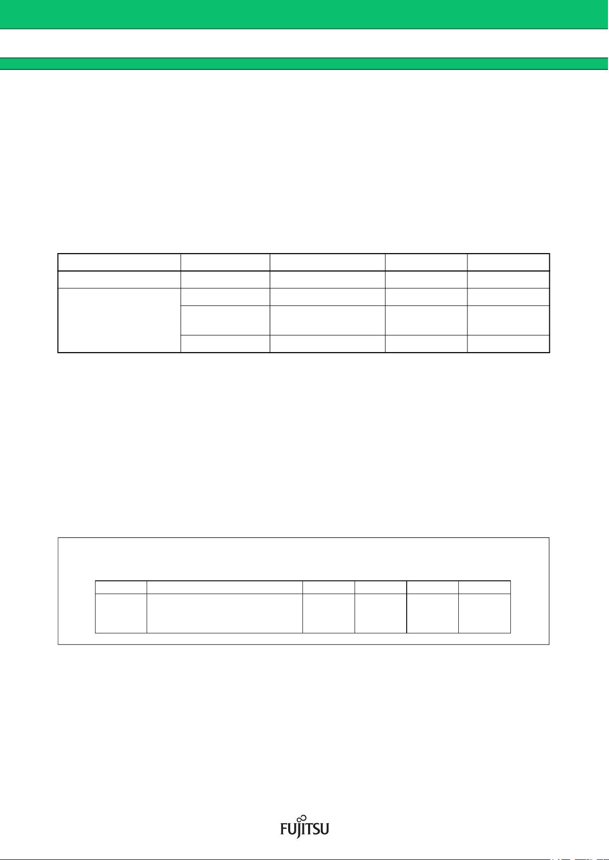
FeRAM Configuration
The FeRAM has 2000 bytes for use as user area and 48 bytes for use as system area.
The FeRAM memory areas consist of a total of 256 blocks (250 blocks of user area and 6 blocks of system
area). Each block can store 64 bits (8 bytes) of data.
The block is the unit used for the writing and reading of FeRAM data. The memory configuration of FeRAM
is shown below.
FeRAM memory configuration
Blocks “00
H” to “F9H” are user area. The user area is defined as an area that can be accessed when the
corresponding block address is specified. On the other hand, Blocks “FAH” to “FFH” are system area. The
system area is defined as an area that can be accessed only with a specific command.
The system area consists of 6 blocks and contains UID, AFI, DSFID, EAS bits, and security status (can write
or cannot write) data for individual block. UID is fixed and cannot be updated. AFI, DSFID, and EAS bits are
written at the factory, and can be updated and locked (disable to write) with commands (Only EAS bit cannot
be locked) .
As shown in above, “FA
H” holds the UID, and “FCH” to “FFH” hold the security status information on individual
user areas.
The configuration of “FBH” to “FFH” blocks is shown below. “FBH” block is used for EAS status, AFI and DSFID
data, the security status data of AFI and DSFID. “FCH” to “FFH” blocks contain block security status data.
* : Reserved for future use
Area Block No. Details Data read Data write
User area (2000 bytes) 00
H to F9H User area Yes Yes
System area (48 bytes)
FAH UID (64 bits) Yes No
FB
H
AFI, DSFID, EAS,
security status
Yes Limited
FC
H to FFH Block security status Yes No
MSB
RFU* DSFID
56 33
32 25
LSB
AFI
81
AFI
Lock
16 9
DSFID
Lock
64 57
EAS
Status
24 17
Status
Status
Structure of “FB
H”

MB89R118C
4 DS411-00001-6v0-E
* : Reserved for future use
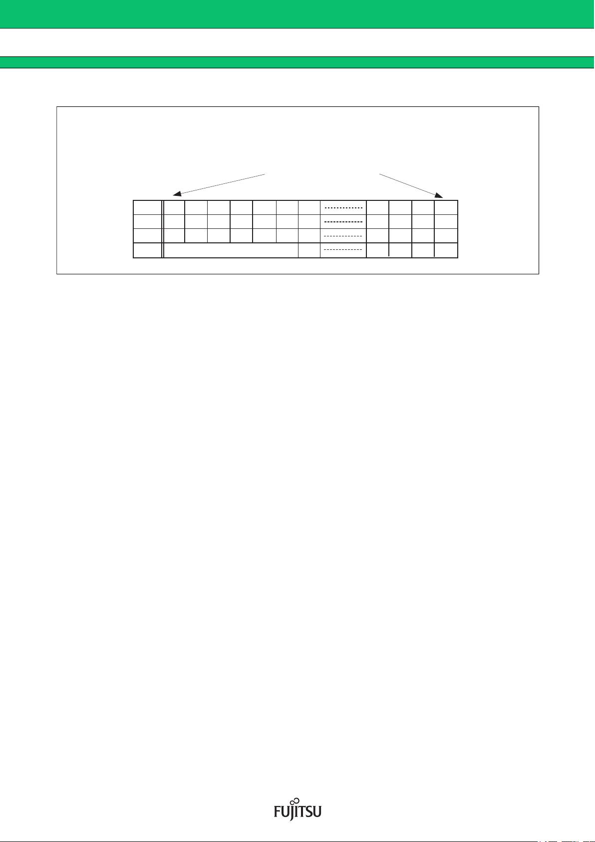
The security status of the user area is stored in the block security status bit in system area blocks of “FCH”
to “FFH” per bit in each block. A user area is unlocked when the corresponding block security status bit is
“0”; it is locked (disable to write state) when the corresponding block security status bit is “1”.
EAS bit is a 1 bit, and it is used for setting EAS status. It is possible to read/write data of 2 blocks at one
time in the user area (If Read Multiple Blocks Unlimited command is used, up to 256 blocks can be accessed
at one time) .
MSB
LSB
FD
H
FC
H
FF
H
FE
H
7F
3F
BF
F9
83
03
43
C3
79
39
B9
7A
3A
BA
7B
3B
BB
7C
3C
BC
7D
3D
BD
7E
3E
BE
82
02
42
C2
81
01
41
C1
80
00
40
C0
RFU* (6 bits)
Block security status (BSS) of user
block 3F
H
Block security status (BSS) of user
block 00
H
Structure of “FCH” to “FFH”

MB89R118C
DS411-00001-6v0-E 5
DATA ELEMENT DEFINITION
1. Unique Identifier (UID)
The MB89R118C has a 64-bit unique identifier (UID). The UID is used to distinguish a transponder from
another transponder in the anti-collision algorithm described later.
The UID consists of the 3 items shown in the following.
An 8-bit data whose value is always “E0
H” (bit 57 to bit 64)
An 8-bit IC manufacturer code whose value is always “08H”, and is defined by ISO/IEC 7816-6/AMI
(bit 49 to bit 56)
Unique 48-bit serial number assigned by FUJITSU SEMICONDUCTOR (bit 1 to bit 48)
Among the unique 48-bit serial number assigned by FUJITSU SEMICONDUCTOR, the 1 byte from bit 41
to bit 48 defines MB89R118C code whose value is “01H”. And the 5 bytes from bit 1 to bit 40 define other
serial number.
Structure of UID
MSB LSB
64 57 56 49 48 41 40 1
“E0
H”
IC manufacturer
code “08H”
“01H” Other serial number
Unique serial number assigned by
FUJITSU SEMICONDUCTOR
剩余46页未读,继续阅读
资源评论

ou18OO2566372
- 粉丝: 39
- 资源: 1
上传资源 快速赚钱
 我的内容管理
展开
 我的资源
快来上传第一个资源
 我的收益 登录查看自己的收益
 我的积分
登录查看自己的积分
 我的C币
登录后查看C币余额
 我的收藏
我的收藏  我的下载
我的下载  下载帮助
下载帮助

 前往需求广场,查看用户热搜
最新资源
- 人力-工伤培训课件 9.工伤预防培训.pptx
- 人力-工伤培训课件 12.职业病预防.pptx
- 人力-工伤培训课件 10.工伤预防知识培训.pptx
- 人力-工伤培训课件 11.工伤预防知识培训2.pptx
- file-devel-5.11-37.el7.x64-86.rpm.tar.gz
- file-libs-5.11-37.el7.x64-86.rpm.tar.gz
- file-static-5.11-37.el7.x64-86.rpm.tar.gz
- 电力通信 系统中运维数据采 集技术的研究与分析.pdf
- filebench-1.4.9.1-3.el7.x64-86.rpm.tar.gz
- filesystem-content-3.2-25.el7.x64-86.rpm.tar.gz
- 航天发射 体系的脆弱性及发展对策.pdf
- finch-2.10.11-9.el7.x64-86.rpm.tar.gz
- finch-devel-2.10.11-9.el7.x64-86.rpm.tar.gz
- finger-0.17-52.el7.x64-86.rpm.tar.gz
- Postman安装文件 64位 版本7.13
- qqbrowser_15.9.2.2196_GA_20250117_124543_1100125299.apk
资源上传下载、课程学习等过程中有任何疑问或建议,欢迎提出宝贵意见哦~我们会及时处理!
点击此处反馈


安全验证
文档复制为VIP权益,开通VIP直接复制
 信息提交成功