


USER'S MANUAL
S5PC100
June, 2009
REV 1.01
Copyright © 2009 Samsung Electronics, Inc. All Rights Reserved

Important Notice
The information in this publication has been carefully
checked and is believed to be entirely accurate at
the time of publication. Samsung assumes no
responsibility, however, for possible errors or
omissions, or for any consequences resulting from
the use of the information contained herein.
Samsung reserves the right to make changes in its
products or product specifications with the intent to
improve function or design at any time and without
notice and is not required to update this
documentation to reflect such changes.
This publication does not convey to a purchaser of
semiconductor devices described herein any license
under the patent rights of Samsung or others.
Samsung makes no warranty, representation, or
guarantee regarding the suitability of its products for
any particular purpose, nor does Samsung assume
any liability arising out of the application or use of
any product or circuit and specifically disclaims any
and all liability, including without limitation any
consequential or incidental damages.
“Typical” parameters can and do vary in different
applications. All operating parameters, including
“Typicals” must be validated for each customer
application by the customer’s technical experts.
Samsung products are not designed, intended, or
authorized for use as components in systems
intended for surgical implant into the body, for other
applications intended to support or sustain life, or for
any other application in which the failure of the
Samsung product could create a situation where
personal injury or death may occur.
Should the Buyer purchase or use a Samsung
product for any such unintended or unauthorized
application, the Buyer shall indemnify and hold
Samsung and its officers, employees, subsidiaries,
affiliates, and distributors harmless against all
claims, costs, damages, expenses, and reasonable
attorney fees arising out of, either directly or
indirectly, any claim of personal injury or death that
may be associated with such unintended or
unauthorized use, even if such claim alleges that
Samsung was negligent regarding the design or
manufacture of said product.
S5PC100 RISC Microprocessor
User’s Manual, Revision 1.01
Publication Number:
All rights reserved. No part of this publication may be reproduced, stored in a retrieval system, or transmitted in
any form or by any means, electric or mechanical, by photocopying, recording, or otherwise, without the prior
written consent of Samsung Electronics.
Samsung Electronics’ microcontroller business has been awarded full ISO-14001
certification (BSI Certificate No. FM24653). All semiconductor products are
designed and manufactured in accordance with the highest quality standards and
objectives.
Samsung Electronics Co., Ltd.
San #24 Nongseo-Dong, Giheung-Gu
Yongin-City, Gyeonggi-Do, Korea
C.P.O. Box #37, Suwon 446-711
TEL: (82)-(31)-209-2659
FAX: (82)-(31)-209-6285
Home Page: http://www.samsungsemi.com
Printed in the Republic of Korea
E-Mail:
mobilesol.cs@samsung.com
S5PC100_UM_REV1.0 iii
Revision History
Revision No. Description Author(s) Date
0.00 Initial Draft (Preliminary spec) AP design November, 2008
0.10
Following chapters are added
- Electrical Data, Mechanical Data
Following chapters are updated
- Overview, Memory map, Chip ID, GPIO, Clock
controller, Power management, Booting sequence,
DRAM controller, SROM controller, OneNAND
controller, NAND Flash controller, DMA controller,
System timer, MIPI DSIM, MIPI CSIS, USB HOST
controller, USB2.0 HS OTG, Modem interface,
SD/MMC controller, Display controller, Camera
interface, JPEG, FIMG-3DSE, TV & Video DAC,
Video Processor, Mixer, HDMI, Multi format codec,
Audio sub system, ADC & Touch screen interface,
Keypad interface, Security system, Advanced
crypto engine
AP design January, 2009
0.20
Unused pin are renamed.
AP Evaluation February, 2009
1.00
Public draft
AP Evaluation May, 2009
1.01
Some chapters are updated
AP Evaluation June, 2009

S5PC100 USER’S MANUAL (REV1.0) PRODUCT OVERVIEW
1.1-1
1.1 PRODUCT OVERVIEW
1 ARCHITECTURAL OVERVIEW
S5PC100 is a 32-bit RISC cost-effective, low power, high performance microprocessor solution for mobile phones
and general applications, and integrates an ARM CortexTM-A8 which implements the ARM architecture V7-A with
supporting numerous peripherals.
To provide optimized Hardware (H/W) performance for the 3G and 3.5G communication services, S5PC100
adopts 64-bit internal bus architecture and includes many powerful hardware accelerators for tasks such as
motion video processing, display control and scaling. Integrated Multi Format Codec (MFC) supports encoding
and decoding of MPEG-1/2/4, H.263, H.264 and decoding of VC1, Divx. This Hardware accelerators support real-
time video conferencing and Analog TV out, HDMI for NTSC and PAL mode
The S5PC100 has an optimized interface to external memory capable of sustaining the demanding memory
bandwidths required in high-end communication services. The memory system has Flash/ ROM external memory
ports for parallel access and DRAM port for high bandwidth. DRAM port can be configured to support mobile
DDR, DDR2 or LPDDR2.
Flash/ROM Port supports NAND Flash, NOR-Flash, OneNAND and ROM type external memory.
To reduce total system cost and enhance overall functionality, S5PC100 includes many hardware peripherals
such as TFT 24-bit true color LCD controller, Camera Interface, MIPI DSI, CSI-2 and HSI, System Manager for
power management, CF+, ATA I/F, 4-channel UART, 24-channel DMA, 4-channel Timers, General I/O Ports, 3-ch
IIS, 1-ch S/PDIF, 2-ch CAN bus, IIC-BUS interface, 3-ch HS-SPI, USB Host v1.1, USB OTG v2.0 operating at
high speed (480Mbps), SD Host & High Speed Multi-Media Card Interface and PLLs for clock generation.
Package on Package (POP) option with MCP is available for small form factor applications.
Salient features of S5PC100 are summarized below:
PRODUCT OVERVIEW S5PC100 USER’S MANUAL (REV1.0)
1.1-2
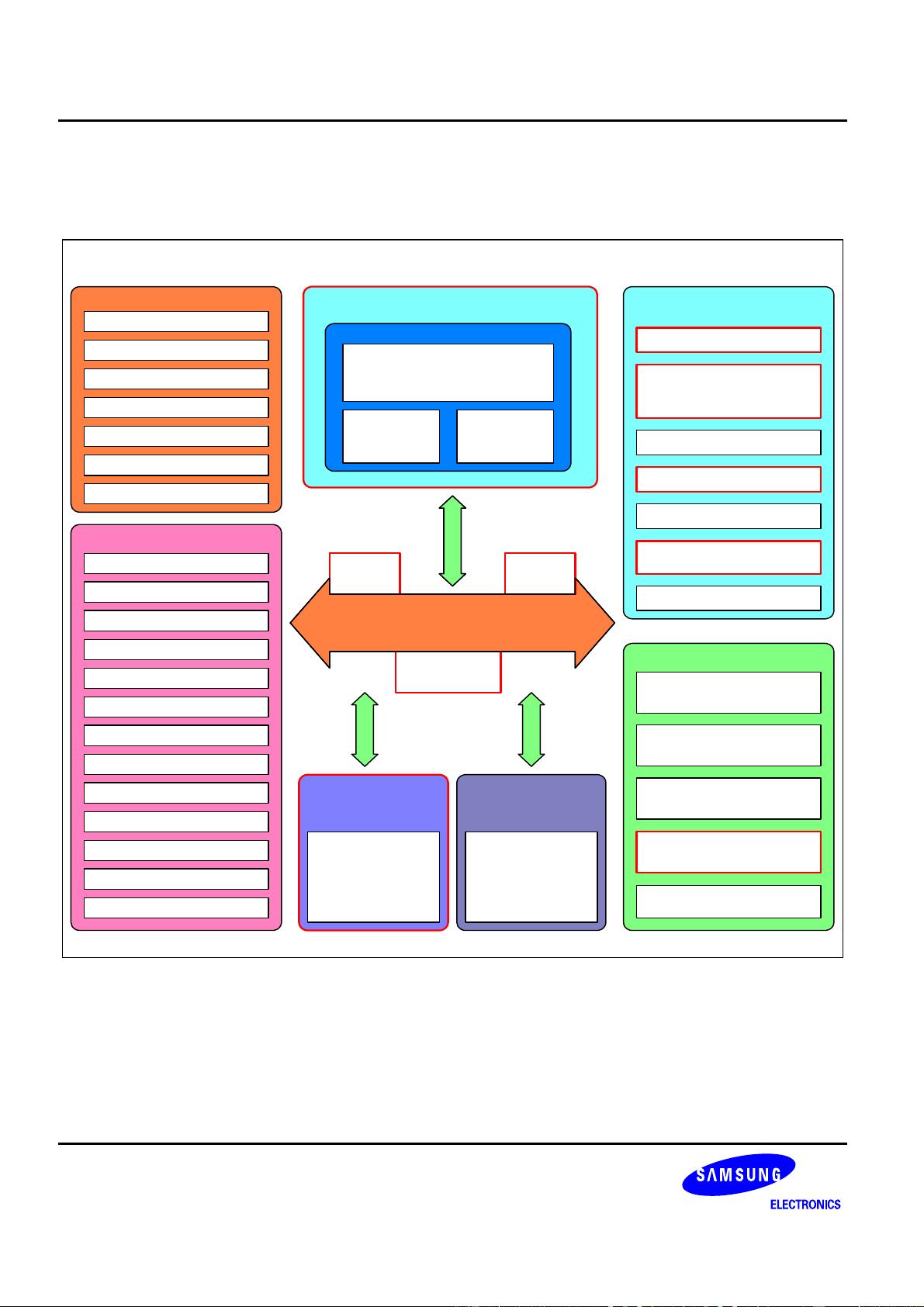
2 BLOCK DIAGRAM
This section summarizes the features of the S5PC100. Figure 1.1- 1 shows an overall block diagram of the
S5PC100.
ARM CoreSystem Peripheral
Connectivity
Multimedia
Acceleration
x64 Multi-Layer AHB/AXI Bus
Memory Subsystem
Power
Management
TFT LCD
Controller / DSI
RTC
PLL x 4
Timer / PWM
Watch Dog Timer
DMA(24ch)
Keypad (8 x 8)
ADC & Touch Screen
I2S (3ch)
AC97/PCM I/F(2ch)
S/PDIF (1ch)
UART (4ch)
IrDA v1.1
I2C(2ch)
HS-SPI (3ch)
MIPI-HSI/Modem I/F
USB Host 1.1 & OTG 2.0
CAN I/F (2ch)
HS-MMC/SD (3ch)
CFII(ATA)
GPIO
32KB/32KB I/D Cache
667MHz @ 1.20 V
256KB
L2 Cache
NEON
Secure
iRAM
Secure
iROM
Crypto
Accelerator
Dynamic Voltage
Frequency Scaling
24/18-bit TFT LCD
8-bit for Dual i80
1024x768 output
5-layer PIP
16-bit a-blending
Camera IF / CSI-2
720p 30fps MFC
Codec - H.263/H.264/MPEG4
Decoder - MPEG2/VC-1/Divx
LCDC/OSD
3D Graphics Engine
2D Graphics Engine
NTSC, PAL TV out
(MIPI DSI/HDMI)
JPEG CODEC
SRAM/ROM/NOR
OneNAND
mDDR / DDR2 /
mDDR2
NAND Flash
OneDRAM
CortexA8
Figure 1.1- 1 S5PC100 Block Diagram


