


RFAXIS INC. CONFIDENTIAL NDA MATERIAL
RFX2401C Single-Chip CMOS RFeIC with PA, LNA, Antenna
Switch and Combined Tx/Rx Transceiver Port
Eval Board Test Summary & Application Notes
11/9/2011
Rev. A.9, 11/9/2011
1

RFAXIS INC. CONFIDENTIAL NDA MATERIAL
RFX2401C RFeIC Key Features and Benefits
11/9/2011
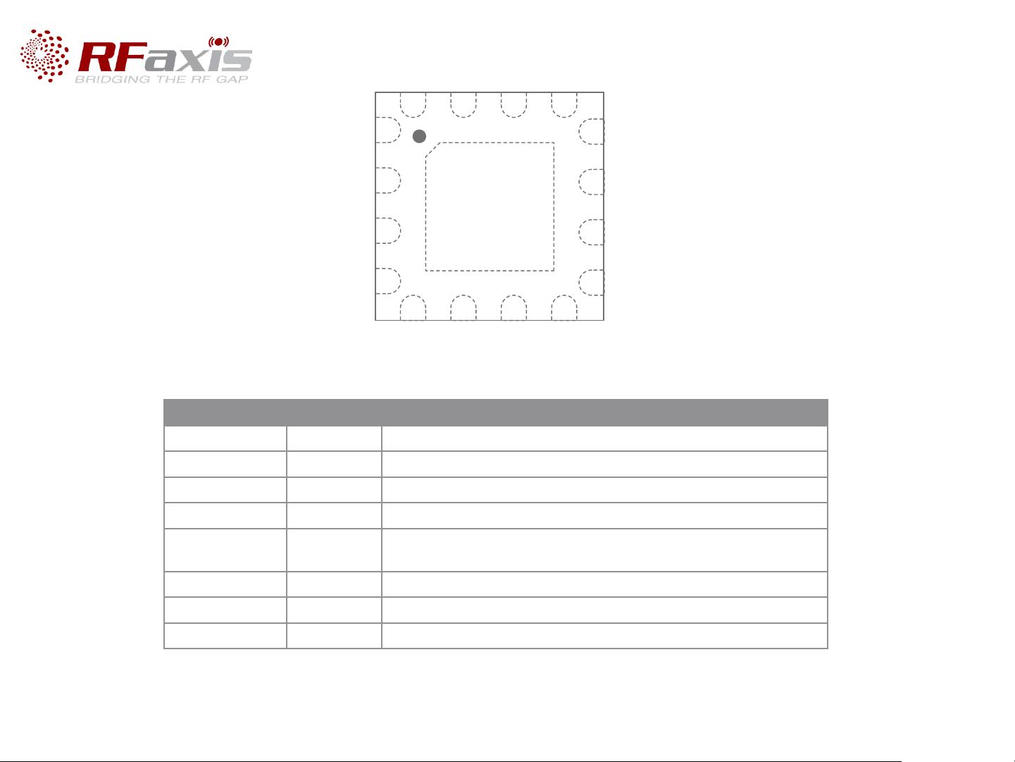
(3x3x0.5mm
16L QFN)
RFX2401C Differentiating Features
Integration of PA, LNA, Tx-Rx Switching Circuitry,
Associated Matching Network, Harmonic Filter,
and PA Power Detection Circuit all into a Single-
Chip, Single-Die pure CMOS Solution
Greatly Reduced and Simplified Tx/Rx Control
Low Voltage Battery Operation down to 2.0V
Digital Logic with 1.2V Turn-On Voltage
No Vref Regulator for Biasing
Common Tx/Rx Port Saves Additional SPDT
Requires Minimal External Components
Small, Ultra-Thin 3x3x0.45mm 16L QFN Package
RFX2401C Customer Benefits
Greatly Simplified, 50 Ohm “Plug & Play” PCB
Implementation
Small Form-Factor and Quick Design Cycle
Simplest Approach to Improve Link Performance
including Range and Receiver Sensitivity
Very Low BOM Cost and Competitive Price
APPLICATIONS
802.15.4 ZigBee Extended Range Devices
ZigBee Smart Power
ZigBee Home Area Network
RF4CE Remote Control
Wireless Sensor Networks
Other 2.4GHz ISM Band Systems
2
GND
GND
1
2
3
4
12
11
10
9
1516 14 13
5 6 7 8
GND
17
GND
GND
GND
GND
DNC
GND
VDD1 VDD2
GND
TXRX
GND
ANT
RXEN
TXEN
RFAXIS INC. CONFIDENTIAL NDA MATERIAL
11/9/2011
RFX2401C Package Pin-Out and Pin Description
3
(Top “See-Through” View)
16
5
1
2
3
4
15 14 13
6 7 8
9
10
11
12
GND
GND
GND
TXRX
TXEN GND
VDD1
GND
GND
ANT
GND
RXEN
GND DNCVDD2
17
GND
GND
Pin Number Pin Name Description
4 TXRX RF signal to/from the Transceiver: DC shorted to GND
5 TXEN CMOS Input to Control TX Enable
6 RXEN CMOS Input to Control RX Enable
10 ANT RF Signal from the PA or RF Signal Applied to the LNA; DC Shorted to GND
1, 2, 3, 7, 8, 9,
11, 12, 15, 17
GND Ground – Must be connected to Ground in the Application Circuit
13 DNC Reserved – Do Not Connect in the Application Circuit
14 VDD2 Voltage Supply Connection for the PA
16 VDD1 Voltage Supply Connection for the LNA

RFAXIS INC. CONFIDENTIAL NDA MATERIAL
11/9/2011
RFX2401C Eval Board and Preliminary BOM
DC Bias & Tx/Rx Logic Control:
VDD=3.3V Nominal (1.8~3.6V Operational)
For Transmit Mode (Tx):
- TXEN=High (>1.2V)
- RXEN= Don’t Care
For Receive Mode (Rx):
- RXEN=High(>1.2V)
- TXEN=Low (<0.3V)
Preliminary BOM:
For VDD decoupling:
C1=10nF (for VDD1, pin 16)
C2=220pF (for VDD2, pin 14)
C3=2.2uF (for both VDD pins)
C4=C5=2pF
L1=1.5nH TDK part # MLG1005S1N5CT000
Eval PCB Information:
- 4-Layer Stack, 10mil/40mil/10mil
- FR4 with er=4.5, tan d = 0.02 (Typ.)
4
Control Logic Truth Table
TXEN RXEN Operating Conditions
1 X TX Active
0 1 RX Active
0 0 Chip is Shut-down
TXEN
RXEN
VDD
GND
ANT
TXRX
C1
C3
C2
C4
C5
L1
RFAXIS INC. CONFIDENTIAL NDA MATERIAL
11/9/2011
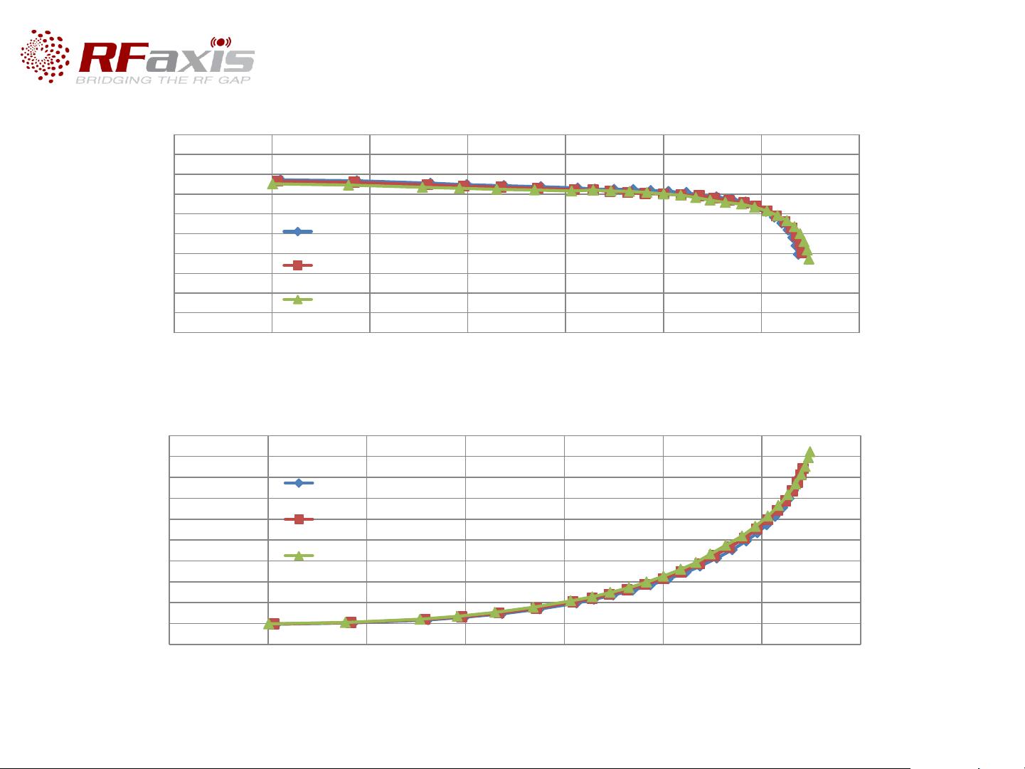
Tx CW Gain and Current vs Pout & Frequency (VDD=3.3V)
5
10
12
14
16
18
20
22
24
26
28
30
-10 -5 0 5 10 15 20 25
Gain [dB]
Pout [dBm]
Gain vs. Pout
2.412GHz
2.45GHz
2.484GHz
0
20
40
60
80
100
120
140
160
180
200
-10 -5 0 5 10 15 20 25
Current [ mA ]
Pout [dBm]
Current vs. Pout
2.412GHz
2.45GHz
2.484GHz
Note: Output power measured at antenna, after the harmonic filter which has ~0.5dB insertion loss.


