没有合适的资源?快使用搜索试试~ 我知道了~
NBP9-用于汽车电池包的压力传感器.pdf
1.该资源内容由用户上传,如若侵权请联系客服进行举报
2.虚拟产品一经售出概不退款(资源遇到问题,请及时私信上传者)
版权申诉
0 下载量 112 浏览量
2023-07-22
15:39:16
上传
评论
收藏 2.36MB PDF 举报
温馨提示
试读
61页
NBP9-用于汽车电池包的压力传感器.pdf
资源推荐
资源详情
资源评论
NBP9
Battery pressure monitor sensor
Rev. 2.4 — 11 March 2022 Product data sheet
1 General description
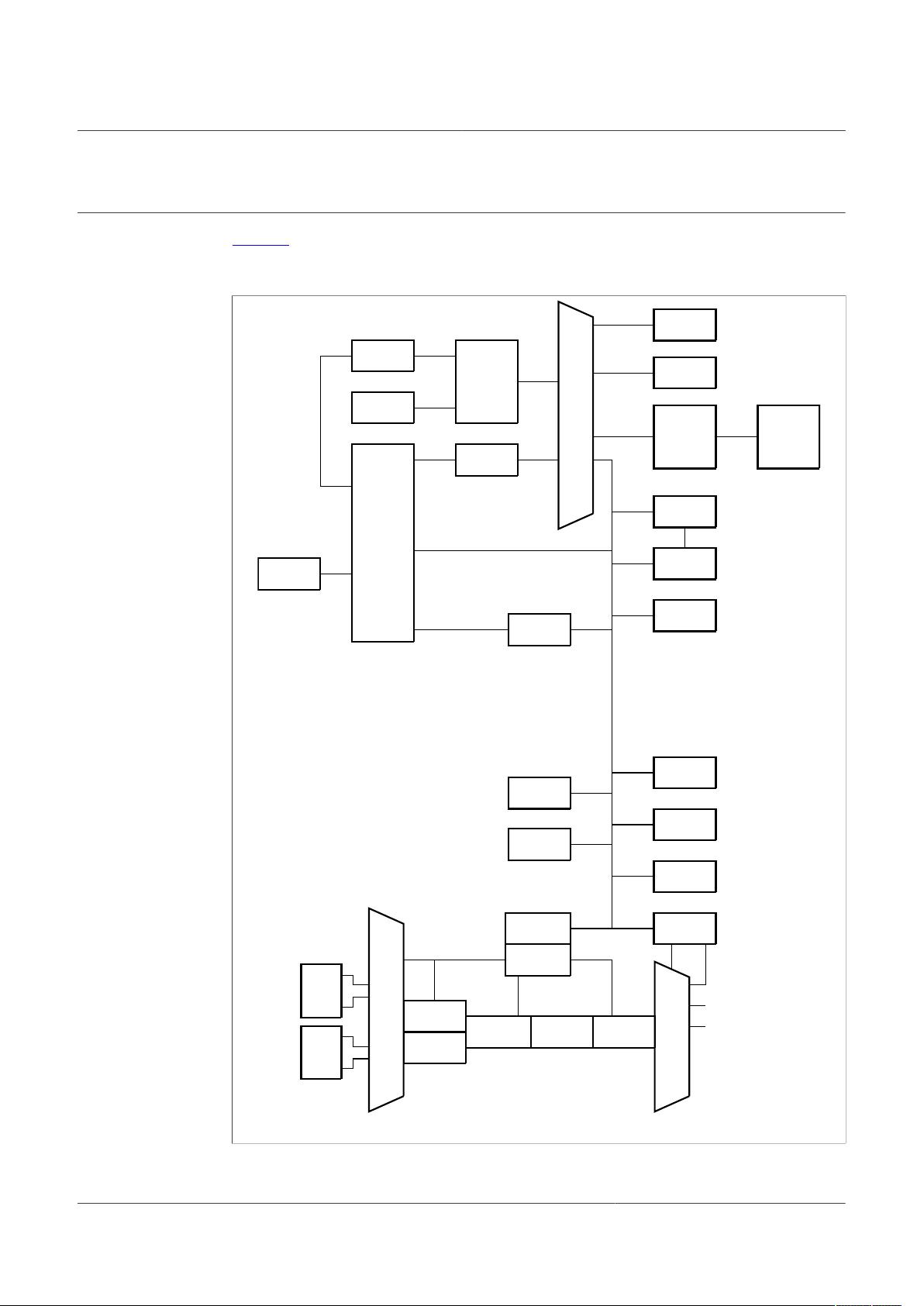
The NBP9 family is a fully integrated battery pressure monitoring sensor (BPMS). The
NBP9 BPMS solution integrates an 8-bit central processing unit (CPU) running on
factory-embedded firmware with serial data and PWM output interfaces to create the
ready-to-use battery pressure monitor sensor.
The NBP9 includes unique autonomous features such as periodic data management with
host notification, pressure change detection with host wake up, and self-test.
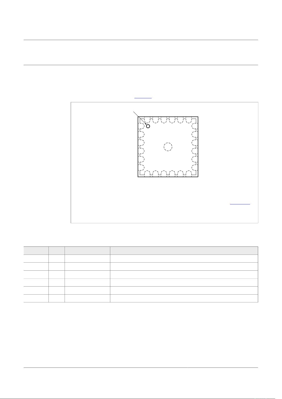
The NBP9 is packaged in a small 4 mm x 4 mm x 1.98 mm wettable-flank QFN, and is
qualified to AEC-Q100 grade 1 and MSL 3 classifications.
2 Features and benefits
• Transducer measurement interfaces with low-power AFE:
– 10-bit compensated pressure sense element
– 8-bit compensated internal device temperature measurement
– 8-bit compensated internal device voltage measurement
• 12-entry pressure FIFO
• Selectable host wake-up indications:
– fixed pressure threshold
– relative pressure threshold
– pressure rate of change threshold
• Client SPI to support host access to internal peripherals, registers, and memory
• Generation of PWM signal encoding error status and pressure measurement
• Qualified in compliance with AEC-Q100, Rev. H
• User-selectable sampling interval
• Low-voltage detection
3 Ordering information
PackageType number
Name Description Version
NBP9 HQFN24 Plastic thermal enhanced quad flat package; no leads, 0.1 dimple wettable flank; 24
terminals; 0.5 mm pitch, 4 mm x 4 mm x 1.98 mm body
SOT1931-1(D)
Table 1. Ordering information
Part Number Pressure Range Pressure tolerances
NBP9FD4T1 40 kPa to 250 kPa Standard tolerances
Table 2. Ordering options
NXP Semiconductors
NBP9
Battery pressure monitor sensor
4 Block diagram
Figure 1 presents the main blocks of the device and their signal interactions. Power
management controls and bus control signals are not shown in this block diagram for
clarity.
aaa-037679
BDM
Controller
S08
8b CPU
Interrupt
Controller
PadMUX
GPIO
IRQ
BKGD
SPI
TPM
ADC
etc.
Pwr. Mode
Controller
Reset
Cntl. Mod.
NV RAM
64 x 8
Sys RAM
512 x 8
Flash
Controller
Flash NVM
16k x 8
System
Int. Mod.
PTA0 - 4
PTB0 - 1
SPI
M0
Bus
Arb.
MUX
S0
S1
S2
S3M1
KeyBd
Interrupt
Int. Clks
Sys
COP
Timer
PWU/RTI
Timer
Peripheral Bus
Free
Run Cntr.
Gain Offset
and Coeff.
Gain Offset
amps
P-cell
Ref.
SAR
ADC
Bandgap
Temp Sensor
SMI
Buffer LPF
2chTPM
Offset
DAC
CtoV
Converter
CtoV
MUX
AtoD
MUX
P-cell
Sns.
Figure 1. Block diagram
NBP9 All information provided in this document is subject to legal disclaimers. © NXP B.V. 2022. All rights reserved.
Product data sheet Rev. 2.4 — 11 March 2022
2 / 61
NXP Semiconductors
NBP9
Battery pressure monitor sensor
5 Pinning information
This section describes the pin layout and general function of each pin.
5.1 Pinning
The device pinout is shown in Figure 2 for the orientation of the pressure port up.
aaa-037680
CGND18
17
16
15
14
13
CGND
PTA1
PTA2
PTA3
PTB0
PTA4 7
8
9
10
11
12
RSTB
VDDA
GND
VDD
n.c.
n
.
c
.
24
23
22
21
20
19
n
.
c
.
P
TB1
n
.
c
.
C
G
N
D
P
T
A
0
n.c.
Pin 1
index area
Transparent top view
1
2
3
4
5
6
n.c.
n.c.
n.c.
n.c.
n.c.
Note: Pins 1-6 are mechanically and electrically connected to the central flag; See Section 12 for
details. If additional ground is desired, any of the pins 1-6 may be routed to circuit board ground
plane, or the central flag may be connected to circuit board ground plane with vias.
Figure 2. Pin configuration
5.2 Pin description
Symbol Pin Function Description
n.c. 1 — Do not connect electrical signals to this pin; solder joint only.
n.c. 2 — Do not connect electrical signals to this pin; solder joint only.
n.c. 3 — Do not connect electrical signals to this pin; solder joint only.
n.c. 4 — Do not connect electrical signals to this pin; solder joint only.
n.c. 5 — Do not connect electrical signals to this pin; solder joint only.
n.c. 6 — Do not connect electrical signals to this pin; solder joint only.
Table 3. Pin description
NBP9 All information provided in this document is subject to legal disclaimers. © NXP B.V. 2022. All rights reserved.
Product data sheet Rev. 2.4 — 11 March 2022
3 / 61
NXP Semiconductors
NBP9
Battery pressure monitor sensor
Symbol Pin Function Description
PTA4 7 PTA4 / BKGD PTA4 Pin - The PTA4 pin places the device in the BACKGROUND DEBUG
mode (BDM) to evaluate CPU code and transfer data to/from the internal
memory. If the BKGD/PTA4 pin is held low when the device comes out of a
power-on-reset (POR), the device switches into the ACTIVE BACKGROUND
DEBUG mode (BDM).
The BKGD/PTA4 pin has an internal pullup device or can be connected to
VDD in the application, unless there is a need to enter BDM operation after
the device as been soldered into the PWB. If in-circuit BDM is desired, the
BKGD/PTA4 pin should be connected to VDD through a resistor (~10 kΩ
or greater) which can be over-driven by an external signal. This resistor
reduces the possibility of inadvertently activating the debug mode in the
application due to an EMC event.
When the application programs port A to GPIOs, PTA4 becomes output-only.
RST_B 8 Reset / V
PP
programming voltage
The RST_B pin is used for test and establishing the BDM condition and
providing the programming voltage source to the internal FLASH memory.
This pin will only be used by customers who intend to reprogram the NBP.
The RST_B pin has an internal pullup device and can be connected to VDD
in the application unless there is a need to enter BDM operation after the
device as been soldered to the PWB. If in-circuit BDM is desired, the RST_B
pin can be left unconnected; but should be connected to VDD through a low
impedance resistor (<10 kΩ) which can be over-driven by an external signal.
This low impedance resistor reduces the possibility of getting into the debug
mode in the application due to an EMC event.
Activation of the external reset function occurs when the voltage on the
RST_B pin goes below 0.3 × V
DD
for at least 100 ns before rising above
0.7 × V
DD
.
VDDA 9 Analog supply The analog circuits operate from a single power supply connected to the unit
through the VDDA pin. VDDA is the positive supply and GND is the ground.
The conductors to the power supply should be connected to the VDDA and
GND pins and locally decoupled.
Care should be taken to reduce measurement signal noise by separating
the VDD, GND, VDDA, and no RFGND pins using a “star” connection such
that each metal trace does not share any load currents with other external
devices.
GND 10 Digital and analog
ground
The digital circuits operate from a single power supply connected to the unit
through the VDD and GND pins. GND is the ground. Care should be taken to
reduce measurement signal noise by separating the GND pins using a “star”
connection such that each metal trace does not share any load currents with
other external devices.
VDD 11 Digital supply The digital circuits operate from a single power supply connected to the unit
through the VDD and GND pins. VDD is the positive supply. The conductors
to the power supply should be connected to the VDD and GND pins and
locally decoupled.
n.c. 12 — Do not connect electrical signals to this pin; solder joint only.
PTB0 13 PTB0 / TPMCH0 /
AD3
The PTB[0] pin is a general-purpose I/O pin. This pin can be configured
as a nominal bidirectional I/O pin with programmable pullup devices. User
software must configure the general-purpose I/O pin (PTB[1:0]) so that they
do not result in “floating” inputs. PTB0 can be mapped to TPM channel 0, or
to ADC channel 3.
Table 3. Pin description...continued
NBP9 All information provided in this document is subject to legal disclaimers. © NXP B.V. 2022. All rights reserved.
Product data sheet Rev. 2.4 — 11 March 2022
4 / 61
NXP Semiconductors
NBP9
Battery pressure monitor sensor
Symbol Pin Function Description
PTA3 14 PTA3 / KBI3 / SOCI The PTA[3] pin is a general-purpose I/O pin. The pulldown devices can only
be activated if the wake-up interrupt capability is enabled. User software
must configure the general-purpose I/O pins so that they do not result in
“floating” inputs. PTA[3] maps to keyboard interrupt function bit [3]. When SPI
is enabled, PTA[3] serves as SOCI.
PTA2 15 PTA2 / KBI2 / SICO The PTA[2] pin is a general-purpose I/O pin. The pulldown devices can only
be activated if the wake-up interrupt capability is enabled. User software
must configure the general-purpose I/O pins so that they do not result in
“floating” inputs. PTA[2] maps to keyboard interrupt function bit [2]. When SPI
is enabled, PTA[2] serves as SICO.
PTA1 16 PTA1 / KBI1 / SCLK The PTA[1] pin is a general-purpose I/O pin. The pulldown devices can only
be activated if the wake-up interrupt capability is enabled. User software
must configure the general-purpose I/O pins so that they do not result in
“floating” inputs. PTA[1] maps to keyboard interrupt function bit [1]. When SPI
is enabled, PTA[1] serves as SCLK
CGND 17 — To be connected to ground by the application.
CGND 18 — To be connected to ground by the application.
PTA0 19 PTA0 / KBI0 / CS_B /
IRQ
The PTA[0] pin is a general-purpose I/O pin. PTA[0] can be configured as a
normal bidirectional I/O pin with programmable pullup or pulldown devices
and/or wake-up interrupt capability. PTA[0] can be configured for external
interrupt (IRQ). The pulldown devices can only be activated if the wake-up
interrupt capability is enabled. User software must configure the general-
purpose I/O pins so that they do not result in “floating” inputs. PTA[0] maps
to keyboard interrupt function bit [0]. When SPI is enabled, PTA0 serves as
CS_B.
CGND 20 — To be connected to ground by the application.
n.c. 21 — Do not connect electrical signals to this pin; solder joint only.
PTB1 22 PTB1 / TPMCH1 /
AD4
The PTB[1] pin is a general-purpose I/O pin. This pin can be configured
as a nominal bidirectional I/O pin with programmable pullup devices. User
software must configure the general-purpose I/O pins (PTB[1:0]) so that they
do not result in “floating” inputs. PTB1 can be mapped to TPM channel 1, or
to ADC channel 4.
n.c. 23 — Do not connect electrical signals to this pin; solder joint only.
n.c. 24 — Do not connect electrical signals to this pin; solder joint only.
Table 3. Pin description...continued
NBP9 All information provided in this document is subject to legal disclaimers. © NXP B.V. 2022. All rights reserved.
Product data sheet Rev. 2.4 — 11 March 2022
5 / 61
剩余60页未读,继续阅读
资源评论
RedCar
- 粉丝: 26
- 资源: 1750
上传资源 快速赚钱
- 我的内容管理 展开
- 我的资源 快来上传第一个资源
- 我的收益 登录查看自己的收益
- 我的积分 登录查看自己的积分
- 我的C币 登录后查看C币余额
- 我的收藏
- 我的下载
- 下载帮助
安全验证
文档复制为VIP权益,开通VIP直接复制
信息提交成功