没有合适的资源?快使用搜索试试~ 我知道了~
Data+Sheet.pdf
需积分: 9 0 下载量 59 浏览量
2022-10-20
11:51:53
上传
评论
收藏 1.1MB PDF 举报
温馨提示
试读
28页
Data+Sheet.pdf
资源详情
资源评论
资源推荐
General Description
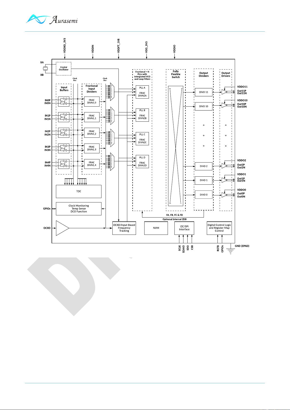
Au5508 offers most integrated 5G clock solution:
Combines BBU, Wireline, AAU, Serdes requirements in
one part definition.
• Unique integration of Sync Features
o Enables Systems with Low Constant
Time Interval Error
o IEEE1588/SyncE/1 PPS full support
• Lower jitter for higher data rate links
• Lower close in noise and JESD204B/C full
support for AAU RF clocks
• Integrated feature rich single part offers
unparalleled flexibility to the system designer
Features
• Ultra Performance PLLs
• Fully Integrated design with no external components
• 120 fs Typical RMS integrated jitter (12k-20M)
• 122.88M Output with excellent close in noise
performance
• Fully Flexible Output and Input Mux: High level of
flexibility in output allocation for PLLs
• JESD204B/C Support for data converter clocks
• 1 PPS Input / Output Support with sub 20s lock time
• External EEPROM Support
• TDC Mode available on all input clocks to measure
input delays with < 10 ps accuracy: 10 TDC Channels
available (independent of the PLLs)
• Frequency Control DCO: DCO Control on all outputs
(down to 1/16 ppt)
• Phase Control DCO: Fine phase adjustment knob for
phase of all outputs from a PLL (adjustment accuracy
< 1ps) in both closed loop and open loop modes
• Internal modes to combine wander of OCXO with
jitter of XO for holdover– Provides 24 hour holdover
with programmable HO accuracy settings
• Best in class hitless switching performance: PBO with
sub 25 ps hit, Phase Propagation & Frequency Ramp
with programmable freq/phase slopes
• Fully integrated Jitter and wander attenuation options
down to 0.09 mHz
• Repeatable input to output delays with output relative
delay adjust
• Internal ZDB Mode with < 0.5 ns Input to Output delay
independently available for each PLL
• Outputs can be phase aligned an independent sync
pulse
• 72 QFN 10mm X 10mm Package
Product
Family
Inputs / Outputs
Input Freq
Output Frequency
RMS Jitter
Packages
55xx
5 Diff / 10 SE Inputs
Up to 12 Diff / 24 SE
Outputs
0.5 Hz - 2.1 GHz
0.5 Hz-
2.94912 GHz
~ 120 fs typ
72 QFN
Au5508: Quad PLL Frequency Translator / Jitter Attenuator / Network
and Port Synchronizer / AAU Clock
Au5508 Short Datasheet
Aura Semiconductor Confidential Rev0.1 Page 3 of 28
Table of Contents
General Description ................................................................................................................................................1
Features ..................................................................................................................................................................1
Table of Contents ...................................................................................................................................................3
List of Tables ..........................................................................................................................................................4
List of Figures .........................................................................................................................................................5
Pin Description .....................................................................................................................................................6
Electrical Characteristics .................................................................................................................................. 10
Functional Description ...................................................................................................................................... 22
Package Information ......................................................................................................................................... 26
Revision History ................................................................................................................................................ 27
Trademarks ....................................................................................................................................................... 27
Contact Information .......................................................................................................................................... 28
Au5508 Short Datasheet
Aura Semiconductor Confidential Rev0.1 Page 4 of 28
List of Tables
Table 1 Pin Description ...........................................................................................................................................6
Table 2 Absolute Maximum Ratings .................................................................................................................... 10
Table 3 Operating Temperature and Thermal Characteristics ............................................................................ 10
Table 4 Input Clock Characteristics ..................................................................................................................... 12
Table 5 Serial Data and Clock Input, GPIOs ....................................................................................................... 13
Table 6 Output Serial and Status Pin .................................................................................................................. 13
Table 7 Output Clock Characteristics .................................................................................................................. 14
Table 8 Fault Monitoring Indicators ..................................................................................................................... 16
Table 9 Crystal Requirements ............................................................................................................................. 17
Table 10 Output RMS Jitter in Frequency Translation Modes ............................................................................ 18
Table 11 Close-In Offset Phase Noise ................................................................................................................ 18
Table 12 Power Supply Rejection ....................................................................................................................... 19
Table 13 Adjacent Output Cross Talk .................................................................................................................. 19
Table 14 Output Clock Specifications .................................................................................................................. 19
Table 15 PIF Description ..................................................................................................................................... 25
Table 16 Revision History .................................................................................................................................... 27
Au5508 Short Datasheet
Aura Semiconductor Confidential Rev0.1 Page 5 of 28
List of Figures
Figure 1 Functional Overview .................................................................................................................................2
Figure 2 Au5508 Pin Configuration ........................................................................................................................6
Figure 3 Au5508 Functional Block Diagram ........................................................................................................ 23
Figure 4 Output Clock Distribution ....................................................................................................................... 24
Figure 5 PLL Internals ......................................................................................................................................... 24
Figure 6 Package Information ............................................................................................................................. 26
剩余27页未读,继续阅读
m0_56681606
- 粉丝: 0
- 资源: 1
上传资源 快速赚钱
- 我的内容管理 展开
- 我的资源 快来上传第一个资源
- 我的收益 登录查看自己的收益
- 我的积分 登录查看自己的积分
- 我的C币 登录后查看C币余额
- 我的收藏
- 我的下载
- 下载帮助
安全验证
文档复制为VIP权益,开通VIP直接复制
信息提交成功
评论0