
A Basic Intro duction to the g
m
/I
D
-Based Design
Methodology
0.1 Abstract
This article introduces the reader to the g
m
/I
D
-based
design methodology, which is a way to help CMOS
analog circuit designers link physical transistor pa-
rameters to small signal models. It is written at the
level of university students who are taking a first
course on analog integrated circuits. It is also rel-
evant to experienced engineers interested in a design
flow that incorporates technology details early in the
design cycle and yields excellent agreement between
hand-calculations and c ircuit simulations.
0.2 Introduction
Following perhaps a long road to maturity, CMOS
has become an excellent platform for analog circuit
design. Not only is it unrivaled in switching and
charge-mode processing, but it benefits from persis-
tent process improvements fueled by the digital con-
sumer marke t. Unfortunately, designers may find it
very di±cult to take advantage of these strengths. A
primary reason for this is that CMOS behavior is hard
to predict without using very complex models, and
this complexity only worsens with technology scal-
ing. Designers, incidentally under pressure to meet
deadlines, are forced to either incorporate complex
models into their hand calculations or spiral into a
Spice-intensive design loop. Neither of these strate-
gies are as eÆective or pleasant as we would like.
My goal in this article is to introduce you to the
g
m
/I
D
-based design methodology, which greatly im-
proves the predictability of CMOS small-signal be-
havior without requiring complex equations. We will
define the ratio g
m
/I
D
in more detail later, but for
now, just think of it as a design variable that encap-
sulates the biasing conditions of a MOS transistor.
Or, even more concisely:
g
m
/I
D
º bias point small-signal model
Development of the methodology will involve several
steps. We will start with a very broad overview of
analog circuit design to see what problem it is that
we are attemping to s olve, and how it has been solved
in the past. I will then explain, at a qualitative level,
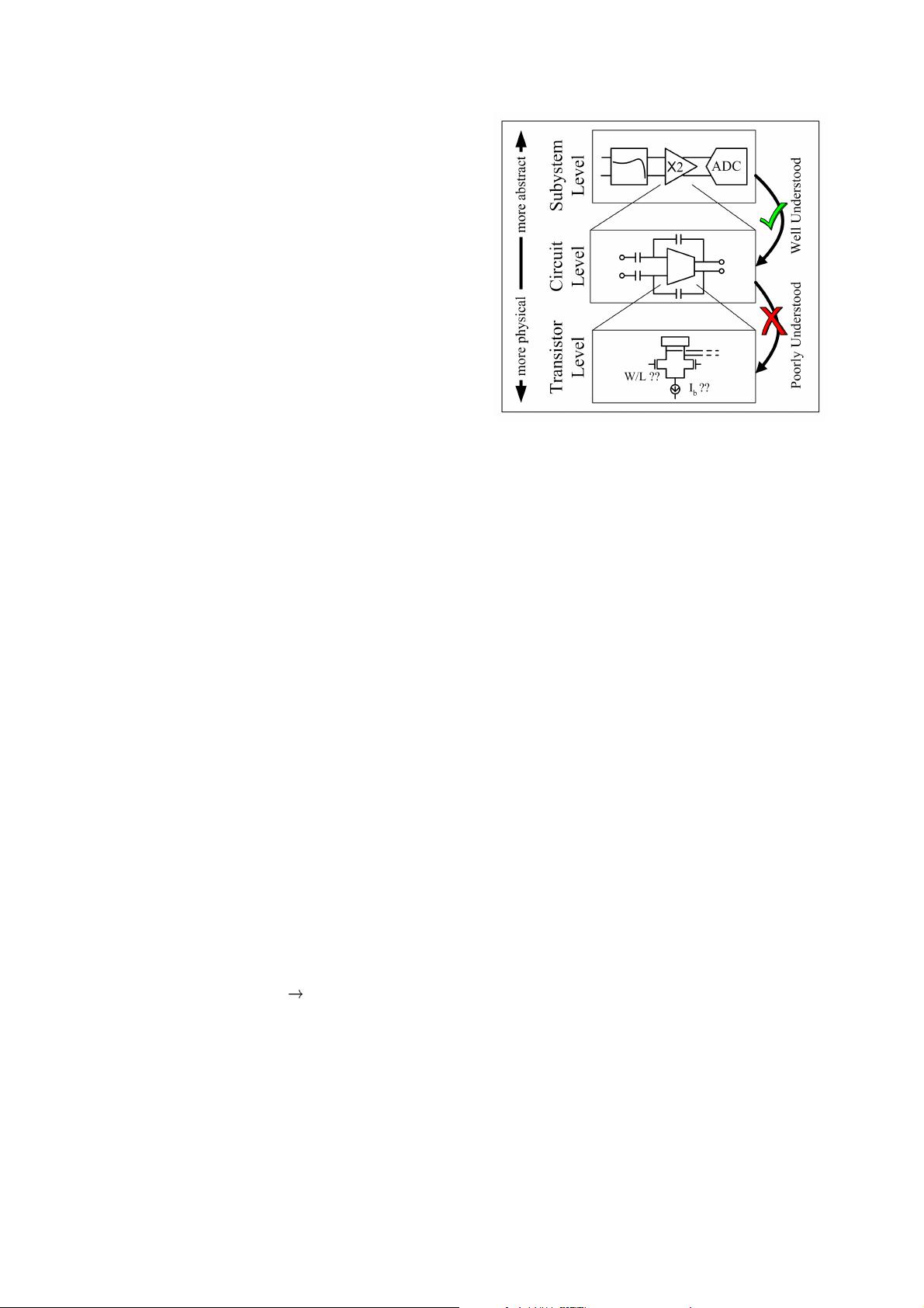
Figure 1: Low-level circuit implementation is often
more di±cult than higher-level design.
why the g
m
/I
D
-based approach is the bes t tool for
solving this problem. Next, we will rehash the en-
tire discussion at a quantitave level. This will entail
a review of transistor operation and a chronological
development of the tools we have available. Finally,
we will close with a thorough design example.
0.3 The Big Picture
0.3.1 Analog Design Relies on Ab-
straction
Fig. 1 shows several levels of abstraction in which we
can view an analog design. Thanks to abstractions,
engineers working at the higher levels can perform
analysis using linear Signals-and-Sytems theory. This
is the domain of filters, gain blocks, OpAmp circuits,
etc. The mathematics that govern this realm are el-
egant, often with centuries-old roots. Consequently,
we have gotten very good at understanding how to
work with these blocks. Most engineering schools
send students through an entire battery of courses
that satisfactorily cover this area.
Descending to the lower levels, there is a diÆerent
story. While we find it straightforward to build a
gain-of-two stage using an OpAmp, we find it very
di±cult to build the OpAmp itself. How big should
each transistor be? How much bias current is needed?
These low-level decisions can be unclear, and there
are two big reasons why. First, transistor behavior
1

剩余14页未读,继续阅读
资源评论


阳眀芓
- 粉丝: 152
- 资源: 2


最新资源
- AI绘画工具介绍(文档)
- pandas-2.2.2-cp311-cp311-musllinux-1-1-aarch64.whl
- 小程序开发基础与简单示例.pdf
- matlab:读取图像+显示图像+显示图像的直方图+直方图均衡
- pandas-2.2.2-cp311-cp311-manylinux-2-17-x86-64.manylinux2014.whl
- 如何充分运用ansys的HELP
- pandas-2.2.2-cp311-cp311-musllinux-1-1-x86-64.whl
- C语言可变长数组(VLA)详解与应用
- android-studio-2024.1.1.12-windows-zip.zip.001
- 辰光PHP客服系统多商户全开源V3.1版+安装教程
资源上传下载、课程学习等过程中有任何疑问或建议,欢迎提出宝贵意见哦~我们会及时处理!
点击此处反馈


