DATA SHEET
Product specification
File under Integrated Circuits, IC17
1999 Apr 12
INTEGRATED CIRCUITS
PCD8544
48 × 84 pixels matrix LCD
controller/driver

1999 Apr 12 2
Philips Semiconductors Product specification
48 × 84 pixels matrix LCD controller/driver PCD8544
CONTENTS
1 FEATURES
2 GENERAL DESCRIPTION
3 APPLICATIONS
4 ORDERING INFORMATION
5 BLOCK DIAGRAM
6 PINNING
6.1 Pin functions
6.1.1 R0 to R47 row driver outputs
6.1.2 C0 to C83 column driver outputs
6.1.3 V
SS1
,V
SS2
: negative power supply rails
6.1.4 V
DD1
,V
DD2
: positive power supply rails
6.1.5 V
LCD1
,V
LCD2
: LCD power supply
6.1.6 T1, T2, T3 and T4: test pads
6.1.7 SDIN: serial data line
6.1.8 SCLK: serial clock line
6.1.9 D/C: mode select
6.1.10 SCE: chip enable
6.1.11 OSC: oscillator
6.1.12 RES: reset
7 FUNCTIONAL DESCRIPTION
7.1 Oscillator
7.2 Address Counter (AC)
7.3 Display Data RAM (DDRAM)
7.4 Timing generator
7.5 Display address counter
7.6 LCD row and column drivers
7.7 Addressing
7.7.1 Data structure
7.8 Temperature compensation
8 INSTRUCTIONS
8.1 Initialization
8.2 Reset function
8.3 Function set
8.3.1 Bit PD
8.3.2 Bit V
8.3.3 Bit H
8.4 Display control
8.4.1 Bits D and E
8.5 Set Y address of RAM
8.6 Set X address of RAM
8.7 Temperature control
8.8 Bias value
8.9 Set V
OP
value
9 LIMITING VALUES
10 HANDLING
11 DC CHARACTERISTICS
12 AC CHARACTERISTICS
12.1 Serial interface
12.2 Reset
13 APPLICATION INFORMATION
14 BONDING PAD LOCATIONS
14.1 Bonding pad information
14.2 Bonding pad location
15 TRAY INFORMATION
16 DEFINITIONS
17 LIFE SUPPORT APPLICATIONS

1999 Apr 12 3
Philips Semiconductors Product specification
48 × 84 pixels matrix LCD controller/driver PCD8544
1 FEATURES
• Single chip LCD controller/driver
• 48 row, 84 column outputs
• Display data RAM 48 × 84 bits
• On-chip:
– Generation of LCD supply voltage (external supply
also possible)
– Generation of intermediate LCD bias voltages
– Oscillator requires no external components (external
clock also possible).
• External
RES (reset) input pin
• Serial interface maximum 4.0 Mbits/s
• CMOS compatible inputs
• Mux rate: 48
• Logic supply voltage range V
DD
to V
SS
: 2.7 to 3.3 V
• Display supply voltage range V
LCD
to V
SS
– 6.0 to 8.5 V with LCD voltage internally generated
(voltage generator enabled)
– 6.0 to 9.0 V with LCD voltage externally supplied
(voltage generator switched-off).
• Low power consumption, suitable for battery operated
systems
• Temperature compensation of V
LCD
• Temperature range: −25 to +70 °C.
2 GENERAL DESCRIPTION
The PCD8544 is a low power CMOS LCD controller/driver,
designed to drive a graphic display of 48 rows and
84 columns. All necessary functions for the display are
provided in a single chip, including on-chip generation of
LCD supply and bias voltages, resulting in a minimum of
external components and low power consumption.
The PCD8544 interfaces to microcontrollers through a
serial bus interface.
The PCD8544 is manufactured in n-well CMOS
technology.
3 APPLICATIONS
• Telecommunications equipment.
4 ORDERING INFORMATION
TYPE NUMBER
PACKAGE
NAME DESCRIPTION VERSION
PCD8544U − chip with bumps in tray; 168 bonding pads + 4 dummy pads −

1999 Apr 12 4
Philips Semiconductors Product specification
48 × 84 pixels matrix LCD controller/driver PCD8544
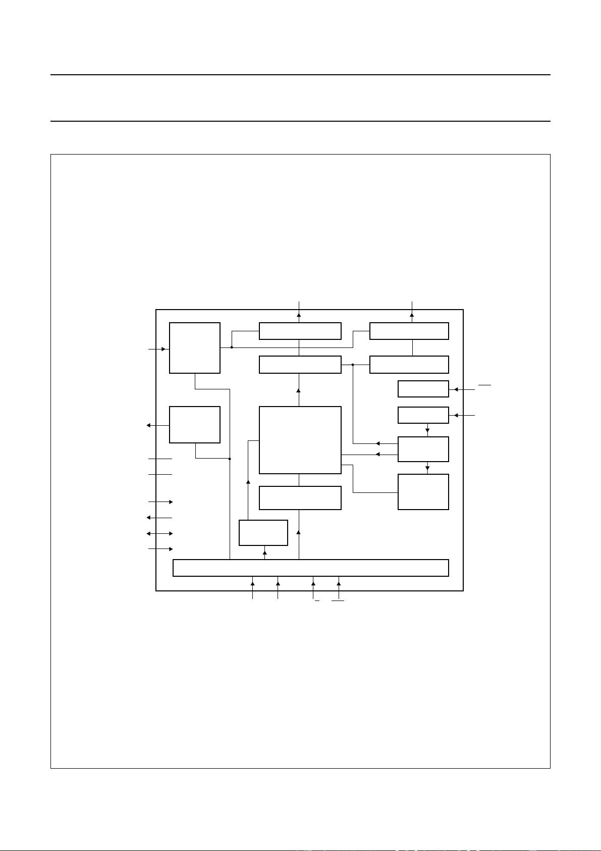
5 BLOCK DIAGRAM
Fig.1 Block diagram.
handbook, full pagewidth
MGL629
COLUMN DRIVERS
DATA LATCHES
DISPLAY DATA RAM
(DDRAM)
48 × 84
ADDRESS COUNTER
DATA
REGISTER
ROW DRIVERS
SHIFT REGISTER
RESET
TIMING
GENERATOR
DISPLAY
ADDRESS
COUNTER
OSCILLATOR
I/O BUFFER
BIAS
VOLTAGE
GENERATOR
V
LCD
GENERATOR
V
LCD2
V
LCD1
V
DD1
to V
DD2
V
SS1
to V
SS2
T2
T1
T3
T4
SCLKSDIN SCED/C
RES
OSC
C1 to C83 R0 to R47
PCD8544

1999 Apr 12 5
Philips Semiconductors Product specification
48 × 84 pixels matrix LCD controller/driver PCD8544
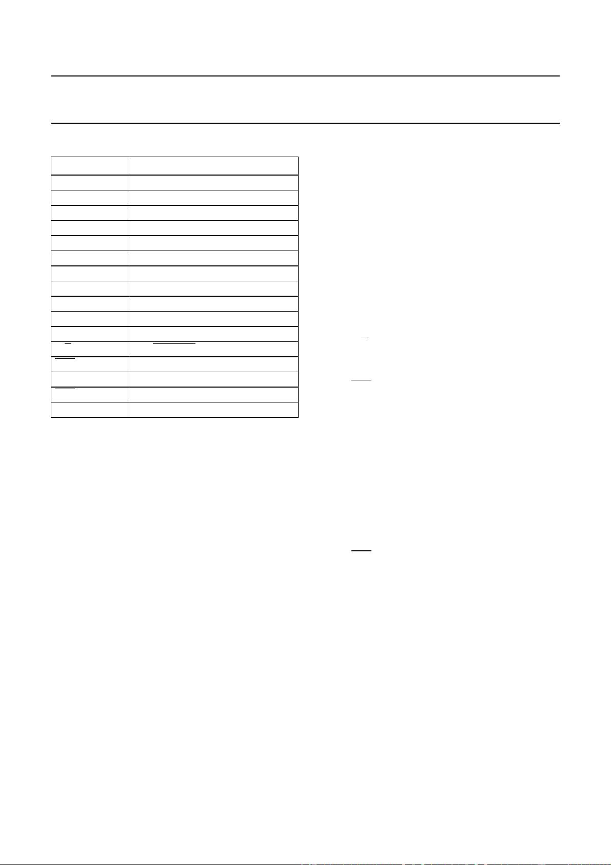
6 PINNING
Note
1. For further details, see Fig.18 and Table 7.
6.1 Pin functions
6.1.1 R0
TO R47 ROW DRIVER OUTPUTS
These pads output the row signals.
6.1.2 C0
TO C83 COLUMN DRIVER OUTPUTS
These pads output the column signals.
6.1.3 V
SS1
,V
SS2
: NEGATIVE POWER SUPPLY RAILS
Supply rails V
SS1
and V
SS2
must be connected together.
6.1.4 V
DD1
,V
DD2
: POSITIVE POWER SUPPLY RAILS
Supply rails V
DD1
and V
DD2
must be connected together.
SYMBOL DESCRIPTION
R0 to R47 LCD row driver outputs
C0 to C83 LCD column driver outputs
V
SS1
,V
SS2
ground
V
DD1
,V
DD2
supply voltage
V
LCD1
,V
LCD2
LCD supply voltage
T1 test 1 input
T2 test 2 output
T3 test 3 input/output
T4 test 4 input
SDIN serial data input
SCLK serial clock input
D/
C data/command
SCE chip enable
OSC oscillator
RES external reset input
dummy1, 2, 3, 4 not connected
6.1.5 V
LCD1
,V
LCD2
: LCD POWER SUPPLY
Positive power supply for the liquid crystal display. Supply
rails V
LCD1
and V
LCD2
must be connected together.
6.1.6 T1, T2, T3
AND T4: TEST PADS
T1, T3 and T4 must be connected to V
SS
, T2 is to be left
open. Not accessible to user.
6.1.7 SDIN:
SERIAL DATA LINE
Input for the data line.
6.1.8 SCLK:
SERIAL CLOCK LINE
Input for the clock signal: 0.0 to 4.0 Mbits/s.
6.1.9 D/
C: MODE SELECT
Input to select either command/address or data input.
6.1.10
SCE: CHIP ENABLE
The enable pin allows data to be clocked in. The signal is
active LOW.
6.1.11 OSC:
OSCILLATOR
When the on-chip oscillator is used, this input must be
connected to V
DD
. An external clock signal, if used, is
connected to this input. If the oscillator and external clock
are both inhibited by connecting the OSC pin to V
SS
, the
display is not clocked and may be left in a DC state.
To avoid this, the chip should always be put into
Power-down mode before stopping the clock.
6.1.12
RES: RESET
This signal will reset the device and must be applied to
properly initialize the chip. The signal is active LOW.


