没有合适的资源?快使用搜索试试~ 我知道了~
L298N英文用户说明书!
4星 · 超过85%的资源 需积分: 11 8 下载量 32 浏览量
2012-06-09
01:06:10
上传
评论
收藏 238KB PDF 举报
温馨提示
试读
12页
L298N英文用户说明书! OPERATINGSUPPLY VOLTAGEUP TO 46 V .TOTAL DC CURRENT UP TO 4 A .LOWSATURATION VOLTAGE .OVERTEMPERATURE PROTECTION LOGICAL ”0” INPUT VOLTAGE UP TO 1.5 V (HIGH NOISE IMMUNITY)
资源推荐
资源详情
资源评论
L298
May 1995
DUAL FULL-BRIDGE DRIVER
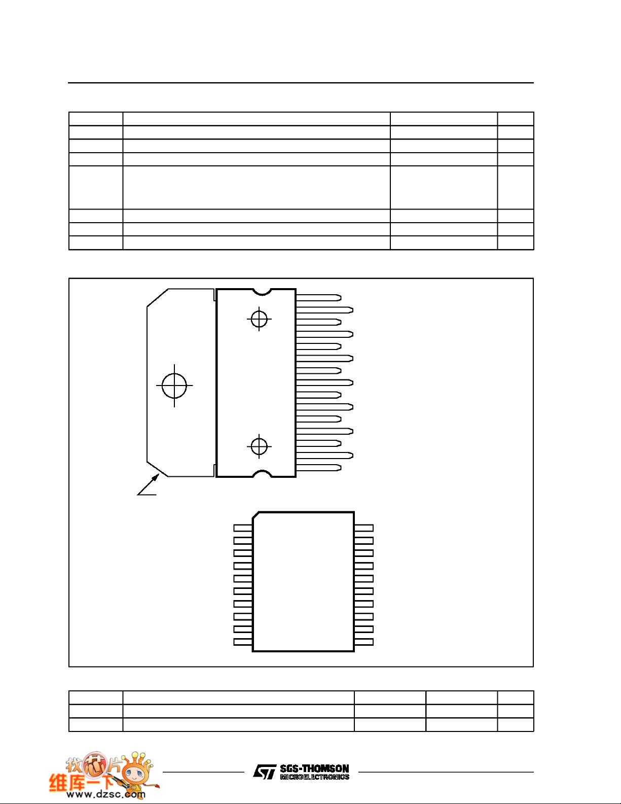
Multiwatt15
ORDERING NUMBERS : L298N (Multiwatt Vert.)
L298HN (Multiwatt Horiz.)
L298P (PowerSO20)
BLOCK DIAGRAM
.OPERATING SUPPLY VOLTAGEUP TO 46 V
.TOTAL DC CURRENT UP TO 4 A
.LOW SATURATION VOLTAGE
.OVERTEMPERATURE PROTECTION
.LOGICAL ”0” INPUT VOLTAGE UP TO 1.5 V
(HIGH NOISE IMMUNITY)
DESCRIPTION
The L298 is an integratedmonolithic circuit in a 15-
lead Multiwatt and PowerSO20 packages. It is a
high voltage, high current dual full-bridge driver de-
signedtoaccept standardTTL logic levels and drive
inductive loads such as relays, solenoids, DC and
steppingmotors. Two enableinputs are provided to
enableor disable thedevice independentlyofthein-
put signals. The emitters of the lower transistors of
each bridge are connected togetherand the corre-
spondingexternalterminal can be used for the con-
nectionofanexternalsensingresistor.Anadditional
supply input is provided so that the logic works at a
lower voltage.
PowerSO20
1/12
PIN CONNECTIONS (top view)
GND
Input 2
VSS
N.C.
Out 1
V
S
Out 2
Input 1
Enable A
Sense A
GND 10
8
9
7
6
5
4
3
2
13
14
15
16
17
19
18
20
12
1
11
GND
D95IN239
Input 3
Enable B
Out 3
Input 4
Out 4
N.C.
Sense B
GND
ABSOLUTE MAXIMUM RATINGS
Symbol Parameter Value Unit
V
S
Power Supply 50 V
V
SS
Logic Supply Voltage 7 V
V
I
,V
en
Input and Enable Voltage –0.3 to 7 V
I
O
Peak Output Current (each Channel)
– Non Repetitive (t = 100µs)
–Repetitive (80% on –20% off; t
on
= 10ms)
–DC Operation
3
2.5
2
A
A
A
V
sens
Sensing Voltage –1 to 2.3 V
P
tot
Total Power Dissipation (T
case
=75°C) 25 W
T
stg
,T
j
Storage and Junction Temperature –40 to 150 °C
THERMAL DATA
Symbol Parameter PowerSO20 Multiwatt15 Unit
R
th j-case
Thermal Resistance Junction-case Max. – 3 °C/W
R
th j-amb
Thermal Resistance Junction-ambient Max. 13 (*) 35 °C/W
(*) Mounted on aluminum substrate
1
2
3
4
5
6
7
9
10
11
8
ENABLE B
INPUT 3
LOGIC SUPPLY VOLTAGE V
SS
GND
INPUT 1
ENABLE A
INPUT 1
SUPPLY VOLTAGE V
S
OUTPUT 2
OUTPUT 1
CURRENT SENSING A
TAB CONNECTED TO PIN 8
13
14
15
12
CURRENT SENSING B
OUTPUT 4
OUTPUT 3
INPUT 4
D95IN240
Multiwatt15
PowerSO20
L298
2/12
PIN FUNCTIONS (refer to the block diagram)
MW.15 PowerSO Name Function
1;15 2;19 Sense A; Sense B Between this pin and ground is connected the sense resistor to
control the current of the load.
2;3 4;5 Out 1; Out 2 Outputs of the Bridge A; the current that flows through the load
connected between these two pins is monitored at pin 1.
46 V
S
Supply Voltage for the Power Output Stages.
A non-inductive 100nF capacitor must be connected between this
pin and ground.
5;7 7;9 Input 1; Input 2 TTL Compatible Inputs of the Bridge A.
6;11 8;14 Enable A; Enable B TTL Compatible Enable Input: the L state disables the bridge A
(enable A) and/or the bridge B (enable B).
8 1,10,11,20 GND Ground.
9 12 VSS Supply Voltage for the Logic Blocks. A100nF capacitor must be
connected between this pin and ground.
10; 12 13;15 Input 3; Input 4 TTL Compatible Inputs of the Bridge B.
13; 14 16;17 Out 3; Out 4 Outputs of the Bridge B. The current that flows through the load
connected between these two pins is monitored at pin 15.
– 3;18 N.C. Not Connected
ELECTRICAL CHARACTERISTICS (V
S
= 42V; V
SS
=5V,T
j
=25°C; unless otherwise specified)
Symbol Parameter Test Conditions Min. Typ. Max. Unit
V
S
Supply Voltage (pin 4) Operative Condition V
IH
+2.5 46 V
V
SS
Logic Supply Voltage (pin 9) 4.5 5 7 V
I
S
Quiescent Supply Current (pin 4) V
en
=H; I
L
=0 V
i
=L
V
i
=H
13
50
22
70
mA
mA
V
en
=L V
i
=X 4 mA
I
SS
Quiescent Current from V
SS
(pin 9) V
en
=H; I
L
=0 V
i
=L
V
i
=H
24
7
36
12
mA
mA
V
en
=L V
i
=X 6 mA
V
iL
Input Low Voltage
(pins 5, 7, 10, 12)
–0.3 1.5 V
V
iH
Input High Voltage
(pins 5, 7, 10, 12)
2.3 VSS V
I
iL
Low Voltage Input Current
(pins 5, 7, 10, 12)
V
i
= L –10 µA
I
iH
High Voltage Input Current
(pins 5, 7, 10, 12)
Vi = H ≤ V
SS
–0.6V 30 100 µA
V
en
= L Enable Low Voltage (pins 6, 11) –0.3 1.5 V
V
en
= H Enable High Voltage (pins 6, 11) 2.3 V
SS
V
I
en
= L Low Voltage Enable Current
(pins 6, 11)
V
en
= L –10 µA
I
en
= H High Voltage Enable Current
(pins 6, 11)
V
en
=H≤V
SS
–0.6V 30 100 µA
V
CEsat (H)
Source Saturation Voltage I
L
=1A
I
L
=2A
1.35
2
1.7
2.7
V
V
V
CEsat (L)
Sink Saturation Voltage I
L
= 1A (5)
I
L
= 2A (5)
1.2
1.7
1.6
2.3
V
V
V
CEsat
Total Drop I
L
= 1A (5)
I
L
= 2A (5)
3.2
4.9
V
V
V
sens
Sensing Voltage (pins 1, 15) –1 (1) 2 V
L298
3/12
剩余11页未读,继续阅读
资源评论
- eyyewardamon2012-10-07勉强可以,太繁杂了
- 伦敦蹦蹦猪2014-06-11勉强可以,太繁杂了
livepor
- 粉丝: 0
- 资源: 2
上传资源 快速赚钱
- 我的内容管理 展开
- 我的资源 快来上传第一个资源
- 我的收益 登录查看自己的收益
- 我的积分 登录查看自己的积分
- 我的C币 登录后查看C币余额
- 我的收藏
- 我的下载
- 下载帮助
最新资源
- MATLAB大数据仿真案例-蚁群算法(ACO)用于求解旅行商(TSP)问题.rar
- MySQL基础知识-个人笔记.rar
- Project8.ipynb
- Python实现BWO-LSTM白鲸算法优化长短期记忆神经网络时间序列预测(完整源码和数据)
- C语言实现文件读写操作的几种常用方法-C 语言.rar
- RK 3568 Android11 版本的梯形校正补丁
- 基于pyqt yolov5 dlib的驾驶员行为监控系统源码+模型.zip
- python代码案例详解-旅行商问题的多种求解算法.rar
- 单相电力电子负载仿真,PWM整流+单相并网逆变
- C语言功能模块(配置文件读取 、debug日志记录等).zip
资源上传下载、课程学习等过程中有任何疑问或建议,欢迎提出宝贵意见哦~我们会及时处理!
点击此处反馈
安全验证
文档复制为VIP权益,开通VIP直接复制
信息提交成功