没有合适的资源?快使用搜索试试~ 我知道了~
资源推荐
资源详情
资源评论
Version 1.3, April 5, 2006 Proprietary to OmniVision Technologies 1
Advanced Information
Preliminary Datasheet
OV7670/OV7171 CMOS VGA (640x480) CAMERACHIP
TM
with OmniPixel
®
Technology
O
mni ision
®
General Description
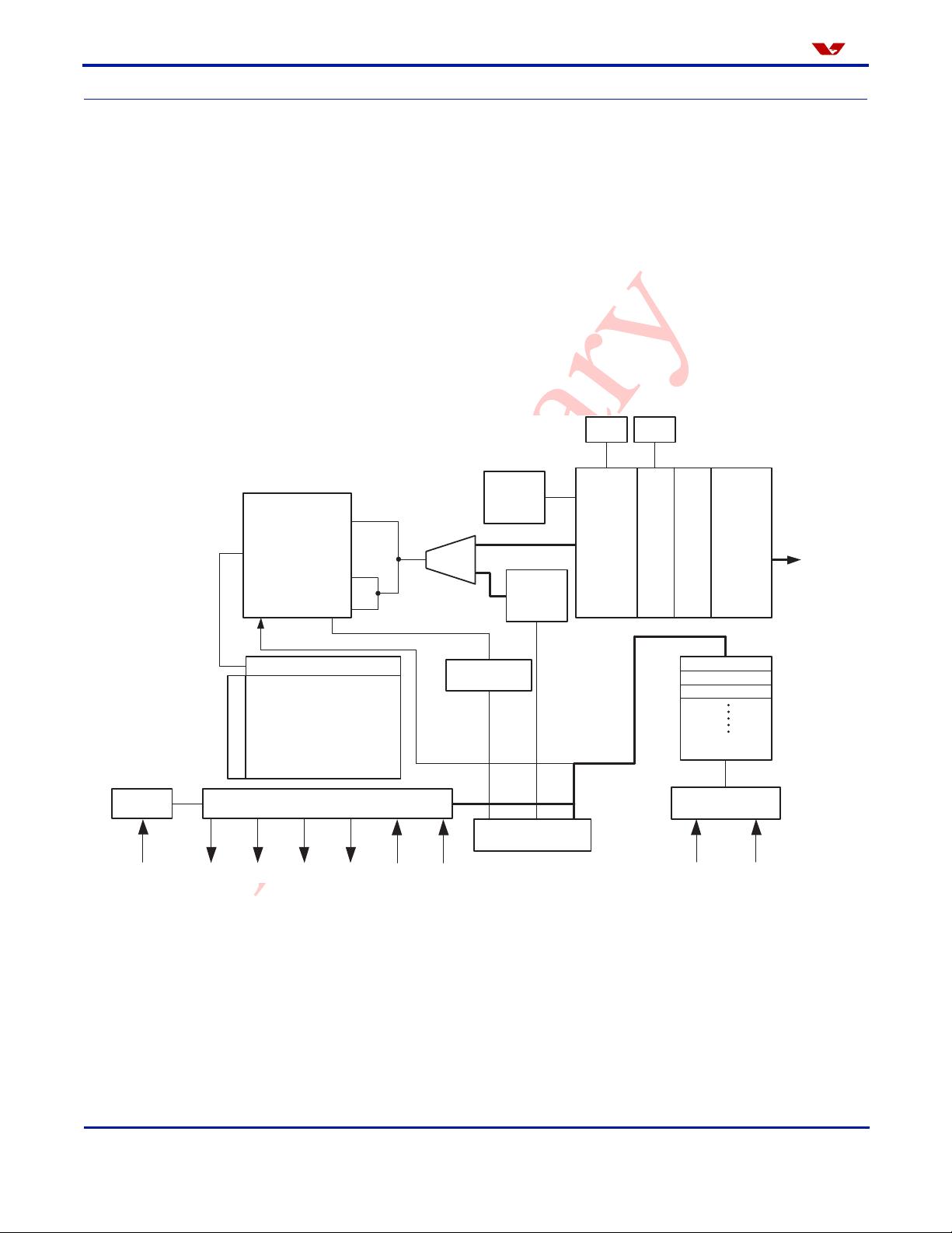
The OV7670/OV7171 CAMERACHIP
TM
is a low voltage CMOS
image sensor that provides the full functionality of a
single-chip VGA camera and image processor in a small
footprint package. The OV7670/OV7171 provides full-frame,
sub-sampled or windowed 8-bit images in a wide range of
formats, controlled through the Serial Camera Control Bus
(SCCB) interface.
This product has an image array capable of operating at up
to 30 frames per second (fps) in VGA with complete user
control over image quality, formatting and output data
transfer. All required image processing functions, including
exposure control, gamma, white balance, color saturation,
hue control and more, are also programmable through the
SCCB interface. In addition, OmniVision C
AMERACHIPs use
proprietary sensor technology to improve image quality by
reducing or eliminating common lighting/electrical sources of
image contamination, such as fixed pattern noise (FPN),
smearing, blooming, etc., to produce a clean, fully stable
color image.
Features
• High sensitivity for low-light operation
• Low operating voltage for embedded portable apps
• Standard SCCB interface compatible with I2C interface
• Output support for Raw RGB, RGB (GRB 4:2:2,
RGB565/555/444), YUV (4:2:2) and YCbCr (4:2:2)
formats
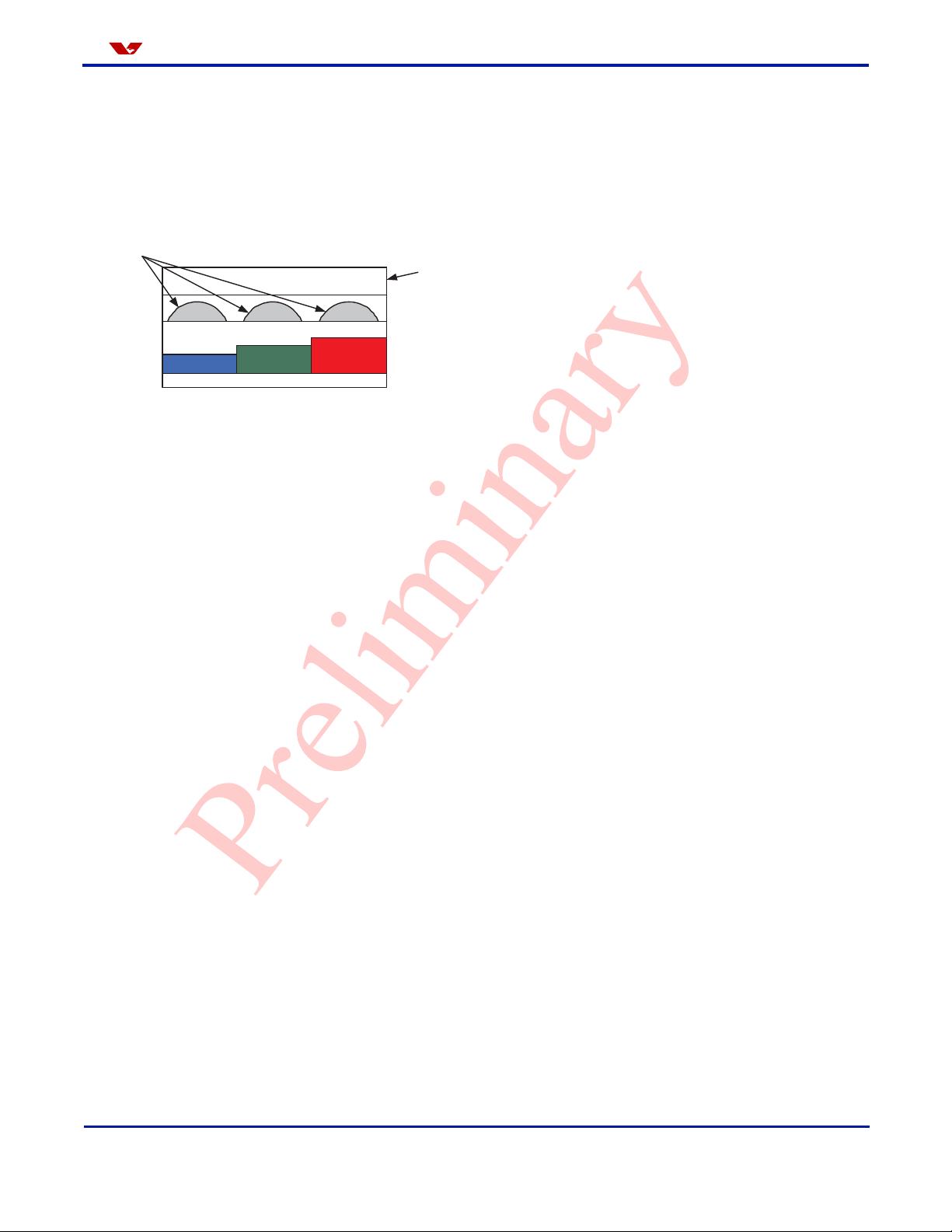
• Supports image sizes: VGA, CIF, and any size scaling
down from CIF to 40x30
•VarioPixel
®
method for sub-sampling
• Automatic image control functions including: Automatic
Exposure Control (AEC), Automatic Gain Control
(AGC), Automatic White Balance (AWB), Automatic
Band Filter (ABF), and Automatic Black-Level
Calibration (ABLC)
• Image quality controls including color saturation, hue,
gamma, sharpness (edge enhancement), and
anti-blooming
• ISP includes noise reduction and defect correction
• Supports LED and flash strobe mode
• Supports scaling
• Lens shading correction
• Flicker (50/60 Hz) auto detection
• Saturation level auto adjust (UV adjust)
• Edge enhancement level auto adjust
• De-noise level auto adjust
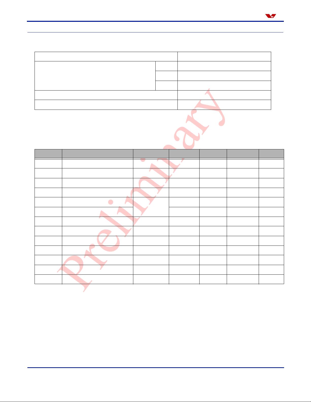
Ordering Information
Pb
Note: The OV7670/OV7171 uses a
lead-free package.
Product Package
OV07670-VL2A (Color, lead-free) 24 pin CSP2
OV07171-VL2A (B&W, lead-free) 24 pin CSP2
Applications
• Cellular and Picture Phones
•Toys
• PC Multimedia
• Digital Still Cameras
Key Specifications
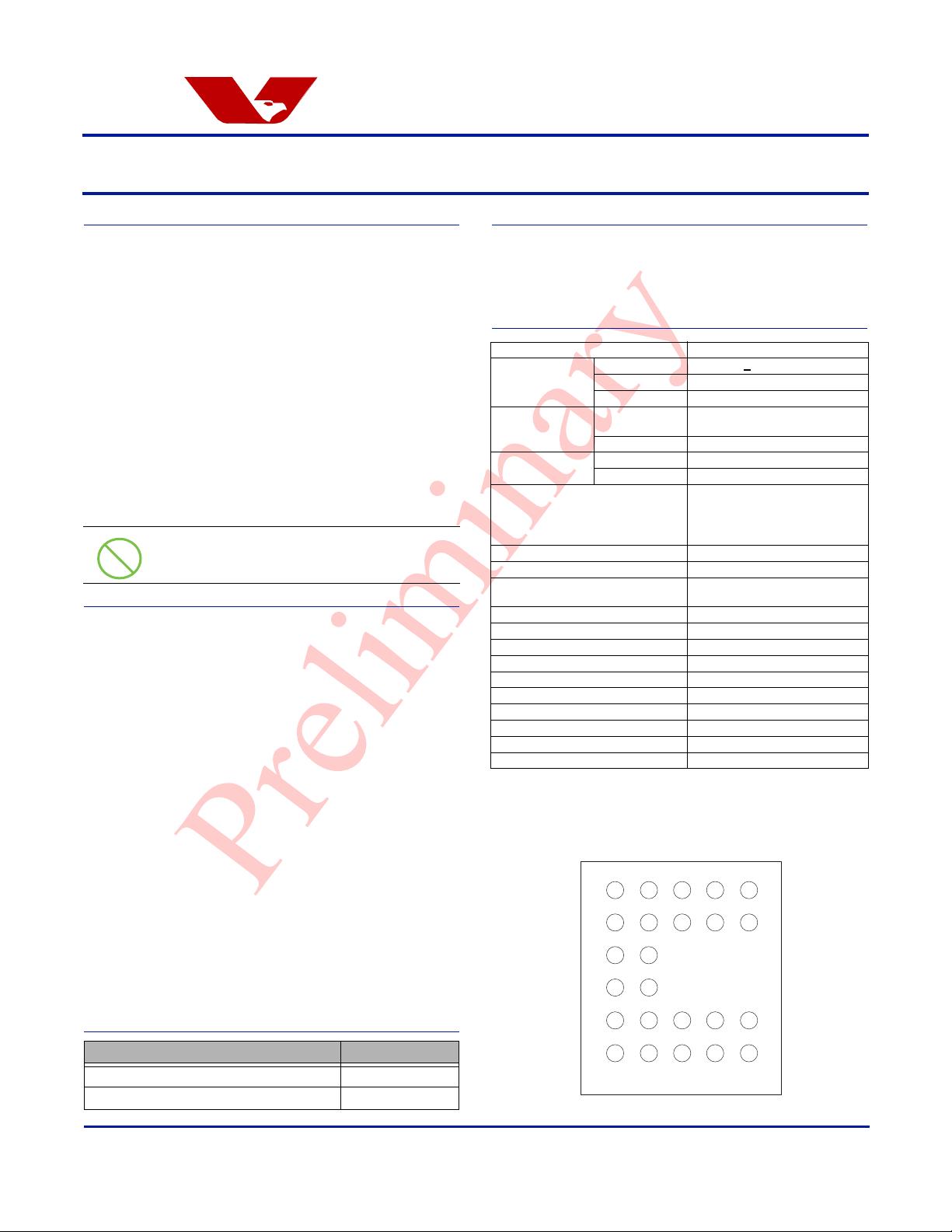
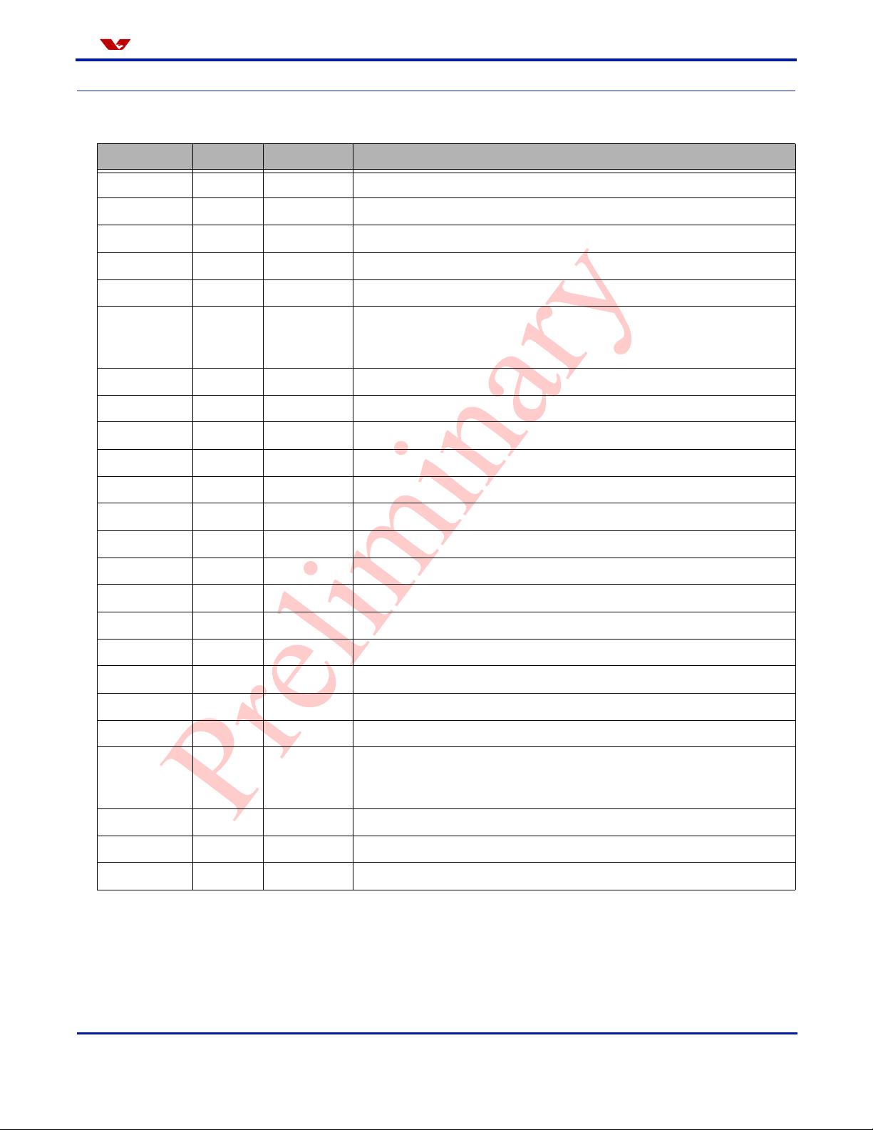
Figure 1 OV7670/OV7171 Pin Diagram (Top View)
Active Array Size 640 x 480
Power Supply
Digital Core 1.8VDC +
10%
Analog 2.45V to 3.0V
I/O 1.7V to 3.0V
a
a. I/O power should be 2.45V or higher when using the internal
regulator for Core (1.8V); otherwise, it is necessary to provide
an external 1.8V for the Core power supply.
Power
Requirements
Active
60 mW typical
(15fps VGA YUV format)
Standby < 20 µA
Temperature
Range
Operation -30°C to 70°C
Stable Image 0°C to 50°C
Output Formats (8-bit)
• YUV/YCbCr 4:2:2
• RGB565/555/444
• GRB 4:2:2
•Raw RGB Data
Lens Size 1/6"
Chief Ray Angle 25°
Maximum Image
Transfer Rate
30 fps for VGA
Sensitivity 1.3 V/(Lux
• sec)
S/N Ratio 46 dB
Dynamic Range 52 dB
Scan Mode Progressive
Electronics Exposure Up to 510:1 (for selected fps)
Pixel Size 3.6 µm x 3.6 µm
Dark Current 12 mV/s at 60°C
Well Capacity 17 K e
Image Area 2.36 mm x 1.76 mm
Package Dimensions 3785 µm x 4235 µm
OV7670/OV7171
AGND
SIO_C
A1
A2 A4
A3
D1
D0
D3
D2
A5
B1
B2 B4
B3
B5
C1
D1
D2
AVDD
SIO_D
PWDN
VSYNC
VREF2
HREF
DVDD
C2
VREF1
D4
D5
E1
E2 E4
E3
E5
F1
F2 F4
F3
F5
DOGNDDOVDD
PCLK STROBE
RESET#
D6
XCLK D7
2 Proprietary to OmniVision Technologies Version 1.3, April 5, 2006
OV7670/OV7171 CMOS VGA (OmniPixel
®
) CAMERACHIP™
O
mni ision
Functional Description
Figure 2 shows the functional block diagram of the OV7670/OV7171 image sensor. The OV7670/OV7171 includes:
• Image Sensor Array (total array of 656 x 488 pixels, with active pixels 640 x 480 in YUV mode)
• Analog Signal Processor
• A/D Converters
• Test Pattern Generator
• Digital Signal Processor (DSP)
• Image Scaler
• Timing Generator
• Digital Video Port
• SCCB Interface
• LED and Strobe Flash Control Output
Figure 2 Functional Block Diagram
A/D
G
D[7:
0]
B
R
50/60 Hz
Auto
Detect
Test
Pattern
Generator
Video
Port
Image
Scaler
DSP
Buffer Buffer
(Lens shading
correction,
de-noise, white/
black pixel
correction, auto
white balance,
etc.)
FIFO
Analog
Processing
Image Array
(656 x 488)
Column Sense Amp
Exposure/Gain
Detect
Exposure/Gain
Control
SCCB
Interface
Registers
Video Timing GeneratorClock
SIO_C SIO_D
STROBE PWDNRESET#VSYNCPCLKHREFXCLK
Row Select
Functional Description
Version 1.3, April 5, 2006 Proprietary to OmniVision Technologies 3
O
mni ision
Image Sensor Array
The OV7670/OV7171 sensor has an image array of
656 x 488 pixels for a total of 320,128 pixels, of which
640 x 480 pixels are active (307,200 pixels). Figure 3
shows a cross-section of the image sensor array.
Figure 3 Image Sensor Array
Timing Generator
In general, the timing generator controls the following
functions:
• Array control and frame generation
• Internal timing signal generation and distribution
• Frame rate timing
• Automatic Exposure Control (AEC)
• External timing outputs (VSYNC, HREF/HSYNC, and
PCLK)
Analog Signal Processor
This block performs all analog image functions including:
• Automatic Gain Control (AGC)
• Automatic White Balance (AWB)
A/D Converters
After the Analog Processing block, the bayer pattern Raw
signal is fed to a 10-bit analog-to-digital (A/D) converter
shared by G and BR channels. This A/D converter
operates at speeds up to 12 MHz and is fully synchronous
to the pixel rate (actual conversion rate is related to the
frame rate).
In addition to the A/D conversion, this block also has the
following functions:
• Digital Black-Level Calibration (BLC)
• Optional U/V channel delay
• Additional A/D range controls
In general, the combination of the A/D Range Multiplier
and A/D Range Control sets the A/D range and maximum
value to allow the user to adjust the final image brightness
as a function of the individual application.
Glas
s
M
icrolens
Blue
Green
Red
Test Pattern Generator
The Test Pattern Generator features the following:
• 8-bar color bar pattern
• Fade-to-gray color bar pattern
• Shift "1" in output pin
Digital Signal Processor (DSP)
This block controls the interpolation from Raw data to
RGB and some image quality control.
• Edge enhancement (a two-dimensional high pass
filter)
• Color space converter (can change Raw data to RGB
or YUV/YCbCr)
• RGB matrix to eliminate color cross talk
• Hue and saturation control
• White/black pixel correction
• De-noise
• Lens shading correction
• Programmable gamma control
• Transfer 10-bit data to 8-bit
Image Scaler
This block controls all output and data formatting required
prior to sending the image out. This block scales
YUV/RGB output from VGA to CIF and almost any size
under CIF.
Digital Video Port
Register bits COM2[1:0] increase I
OL
/I
OH
drive current
and can be adjusted as a function of the customer’s
loading.
SCCB Interface
The Serial Camera Control Bus (SCCB) interface controls
the C
AMERACHIP operation. Refer to OmniVision
Technologies Serial Camera Control Bus (SCCB)
Specification for detailed usage of the serial control port.
LED and Strobe Flash Control Output
The OV7670/OV7171 has a Strobe mode that allows it to
work with an external flash and LED.
Pin Description
Version 1.3, April 5, 2006 Proprietary to OmniVision Technologies 4
O
mni ision
Pin Description
Table 1 Pin Description
Pin Number Name Pin Type Function/Description
A1 AVDD Power Analog power supply
A2 SIO_D I/O SCCB serial interface data I/O
A3 SIO_C Input SCCB serial interface clock input
A4 D1
a
a. D[7:0] for 8-bit YUV or RGB (D[7] MSB, D[0] LSB)
Output YUV/RGB video component output bit[1]
A5 D3 Output YUV/RGB video component output bit[3]
B1 PWDN Input (0)
b
b. Input (0) represents an internal pull-down resistor.
Power Down Mode Selection
0: Normal mode
1: Power down mode
B2 VREF2 Reference Reference voltage - connect to ground using a 0.1 µF capacitor
B3 AGND Power Analog ground
B4 D0 Output YUV/RGB video component output bit[0]
B5 D2 Output YUV/RGB video component output bit[2]
C1 DVDD Power Power supply (+1.8 VDC) for digital logic core
C2 VREF1 Reference Reference voltage - connect to ground using a 0.1 µF capacitor
D1 VSYNC Output Vertical sync output
D2 HREF Output HREF output
E1 PCLK Output Pixel clock output
E2 STROBE Output LED/strobe control output
E3 XCLK Input System clock input
E4 D7 Output YUV/RGB video component output bit[7]
E5 D5 Output YUV/RGB video component output bit[5]
F1 DOVDD Power Digital power supply for I/O (1.7V ~ 3.0V)
F2 RESET# Input
Clears all registers and resets them to their default values.
0: Reset mode
1: Normal mode
F3 DOGND Power Digital ground
F4 D6 Output YUV/RGB video component output bit[6]
F5 D4 Output YUV/RGB video component output bit[4]
5 Proprietary to OmniVision Technologies Version 1.3, April 5, 2006
OV7670/OV7171 CMOS VGA (OmniPixel
®
) CAMERACHIP™
O
mni ision
Electrical Characteristics
NOTE: Exceeding the Absolute Maximum ratings shown above invalidates all AC and DC electrical specifications and may
result in permanent device damage.
Table 2 Absolute Maximum Ratings
Ambient Storage Temperature -40ºC to +95ºC
Supply Voltages (with respect to Ground)
V
DD-A
4.5 V
V
DD-C
3 V
V
DD-IO
4.5 V
All Input/Output Voltages (with respect to Ground) -0.3V to V
DD-IO
+0.5V
Lead-free Temperature, Surface-mount process 245ºC
Table 3 DC Characteristics (-30°C < T
A
< 70°C)
Symbol Parameter Condition Min Typ Max Unit
V
DD-A
DC supply voltage – Analog – 2.45 2.75 3.0 V
V
DD-C
DC supply voltage – Digital Core – 1.62 1.8 1.98 V
V
DD-IO
DC supply voltage – I/O power – 1.7 – 3.0V V
I
DDA
Active (Operating) Current See Note
a
a. V
DD-A
= 2.5V, V
DD-C
= 1.8V, V
DD-IO
= 2.5V
I
DDA
= ∑{I
DD-IO
+ I
DD-C
+ I
DD-A
}, f
CLK
= 24MHz at 30 fps YUV output, no I/O loading
10 + 8
b
b. I
DD-C
= 10mA, I
DD-A
= 8mA, without loading
mA
I
DDS-SCCB
Standby Current
See Note
c
c. V
DD-A
= 2.5V, V
DD-C
= 1.8V, V
DD-IO
= 2.5V
I
DDS-SCCB
refers to a SCCB-initiated Standby, while I
DDS-PWDN
refers to a PWDN pin-initiated Standby
1mA
I
DDS-PWDN
Standby Current 10 20 µA
V
IH
Input voltage HIGH CMOS 0.7 x V
DD-IO
V
V
IL
Input voltage LOW 0.3 x V
DD-IO
V
V
OH
Output voltage HIGH CMOS 0.9 x V
DD-IO
V
V
OL
Output voltage LOW 0.1 x V
DD-IO
V
I
OH
Output current HIGH See Note
d
d. Standard Output Loading = 25pF, 1.2KΩ
8mA
I
OL
Output current LOW 15 mA
I
L
Input/Output Leakage GND to V
DD-IO
± 1 µA
剩余41页未读,继续阅读
资源评论
- meilinfeng2012-12-06啥也没有 毫无价值
- lovelymnk2013-10-04没法用于开发驱动程序。
- herich82013-03-12还可以,对OV2643有帮助
- binliang052014-04-02对了解OV7725有帮助
- baiyabin2014-04-16还是挺有用的
liuxd3000
- 粉丝: 325
- 资源: 32
上传资源 快速赚钱
- 我的内容管理 展开
- 我的资源 快来上传第一个资源
- 我的收益 登录查看自己的收益
- 我的积分 登录查看自己的积分
- 我的C币 登录后查看C币余额
- 我的收藏
- 我的下载
- 下载帮助
安全验证
文档复制为VIP权益,开通VIP直接复制
信息提交成功