HCF4011B.pdf
需积分: 10 115 浏览量
2012-12-20
14:59:31
上传
评论
收藏 342KB PDF 举报


HCC4011B/12B/23B
HCF4011B/12B/23B
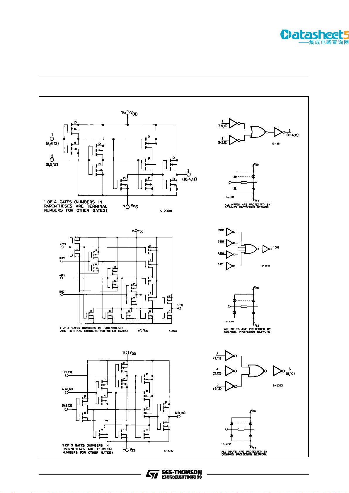
NAND GATES
DESCRIPTION
.PROPAGATION DELAY TIME = 60ns (typ.) AT
C
L
= 50pF, V
DD
= 10V
.BUFFERED INPUTS AND OUTPUTS
.QUIESCENT CURRENT SPECIFIED TO 20V
FOR HCC DEVICE
.INPUT CURRENTOF 100nA AT 18V AND 25°C
FOR HCC DEVICE
.100% TESTED FOR QUIESCENT CURRENT
.5V, 10V AND 15V PARAMETRIC RATINGS
.MEETS ALL REQUIREMENTS OF JEDECTEN-
TATIVE STANDARD N
o
. 13A, ”STANDARD
SPECIFICATIONS FOR DESCRIPTION OF ”B”
SERIES CMOS DEVICES”
QUAD 2 INPUT HCC/HCF 4011B
DUAL 4 INPUT HCC/HCF 4012B
TRIPLE 3 INPUT HCC/HCF 4023B
June 1989
The HCC4011B, HCC4012B and HCC4023B (ex-
tended temperature range) and HCF4011B,
HCF4012B and HCF4023B (intermediate tempera-
ture range) are monolithic, integrated circuit, avail-
able in 14-lead dual in-line plastic or ceramic
package and plastic micropackage.
The HCC/HCF4011B, HCC/HCF4012B and
HCC/HCF4023B NAND gates provide the system
designer with direct implementation of the NAND
function and supplement the existing family of
COS/MOS gates. All inputs and outputs are buf-
fered.
PIN CONNECTIONS
EY
(Plastic Package)
F
(Ceramic Frit Seal Package)
M1
(Micro Package)
C1
(Plastic Chip Carrier)
ORDER CODES :
HCC40XXBF HCF40XXBM1
HCF40XXBEY HCF40XXBC1
4011B 4012B 4023B
1/12
剩余12页未读,继续阅读


评论0
最新资源