C514082_数字信号处理器(DSP-DSC)_规格书(美国微芯)单片机(MCU_MPU_SOC)规格书.PDF
需积分: 1 52 浏览量
2023-09-20
11:14:08
上传
评论
收藏 2.93MB PDF 举报


2013-2017 Microchip Technology Inc. DS70005127D-page 1
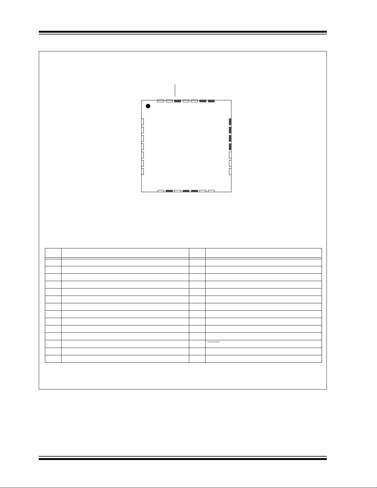
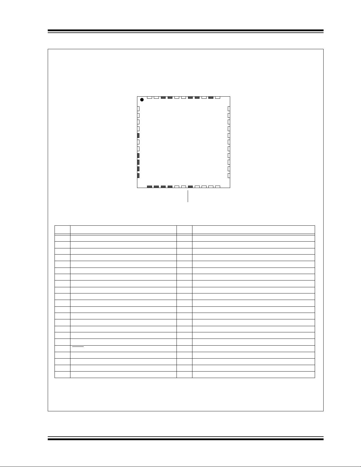
dsPIC33EPXXGS50X FAMILY
Operating Conditions
• 3.0V to 3.6V, -40°C to +85°C, DC to 70 MIPS
• 3.0V to 3.6V, -40°C to +125°C, DC to 60 MIPS
Flash Architecture
• Dual Partition Flash Program Memory with
Live Update (64-Kbyte devices):
- Supports programming while operating
- Supports partition soft swap
Core: 16-Bit dsPIC33E CPU
• Code-Efficient (C and Assembly) Architecture
• Two 40-Bit Wide Accumulators
• Single-Cycle (MAC/MPY) with Dual Data Fetch
• Single-Cycle Mixed-Sign MUL Plus
Hardware Divide
• 32-Bit Multiply Support
• Two Additional Working Register Sets (reduces
context switching)
Clock Management
• ±0.9% Internal Oscillator
• Programmable PLLs and Oscillator Clock Sources
• Fail-Safe Clock Monitor (FSCM)
• Independent Watchdog Timer (WDT)
• Fast Wake-up and Start-up
Power Management
• Low-Power Management modes (Sleep,
Idle, Doze)
• Integrated Power-on Reset and Brown-out Reset
• 0.5 mA/MHz Dynamic Current (typical)
•10 μA I
PD
Current (typical)
High-Speed PWM
• Five PWM Generators (two outputs per generator)
• Individual Time Base and Duty Cycle for each PWM
• 1.04 ns PWM Resolution (frequency, duty cycle,
dead time and phase)
• Supports Center-Aligned, Redundant, Complementary
and True Independent Output modes
• Independent Fault and Current-Limit Inputs
• Output Override Control
• PWM Support for AC/DC, DC/DC, Inverters, PFC
and Lighting
Advanced Analog Features
• High-Speed ADC module:
- 12-bit with 4 dedicated SAR ADC cores and
one shared SAR ADC core
- Configurable resolution (up to 12-bit) for each
ADC core
- Up to 3.25 Msps conversion rate per channel
at 12-bit resolution
- 12 to 22 single-ended inputs
- Dedicated result buffer for each analog channel
- Flexible and independent ADC trigger sources
- Two digital comparators
- Two oversampling filters for increased
resolution
• Four Rail-to-Rail Comparators with Hysteresis:
- Dedicated 12-bit Digital-to-Analog Converter
(DAC) for each analog comparator
- Up to two DAC reference outputs
- Up to two external reference inputs
• Two Programmable Gain Amplifiers:
- Single-ended or independent ground reference
- Five selectable gains (4x, 8x, 16x, 32x and 64x)
- 40 MHz gain bandwidth
Interconnected SMPS Peripherals
• Reduces CPU Interaction to Improve Performance
• Flexible PWM Trigger Options for
ADC Conversions
• High-Speed Comparator Truncates PWM
(15 ns typical):
- Supports Cycle-by-Cycle Current mode control
- Current Reset mode (variable frequency)
Timers/Output Compare/Input Capture
• Five 16-Bit and up to Two 32-Bit Timers/Counters
• Four Output Compare (OC) modules, Configurable
as Timers/Counters
• Four Input Capture (IC) modules
16-Bit Digital Signal Controllers for Digital Power Applications with
Interconnected High-Speed PWM, ADC, PGA and Comparators

剩余389页未读,继续阅读
资源评论


