RDA5802N datasheet_v2.pdf

Copyright © RDA Microelectronics Inc. 2006. All rights are reserved.
The information contained herein is the exclusive property of RDA and shall not be distributed, reproduced, or disclosed in whole or in
part without prior written permission of RDA.
RDA5802N/NS/NM
SINGLE-CHIP BROADCAST FM RADIO TUNER Rev.2.0–Mar.2011
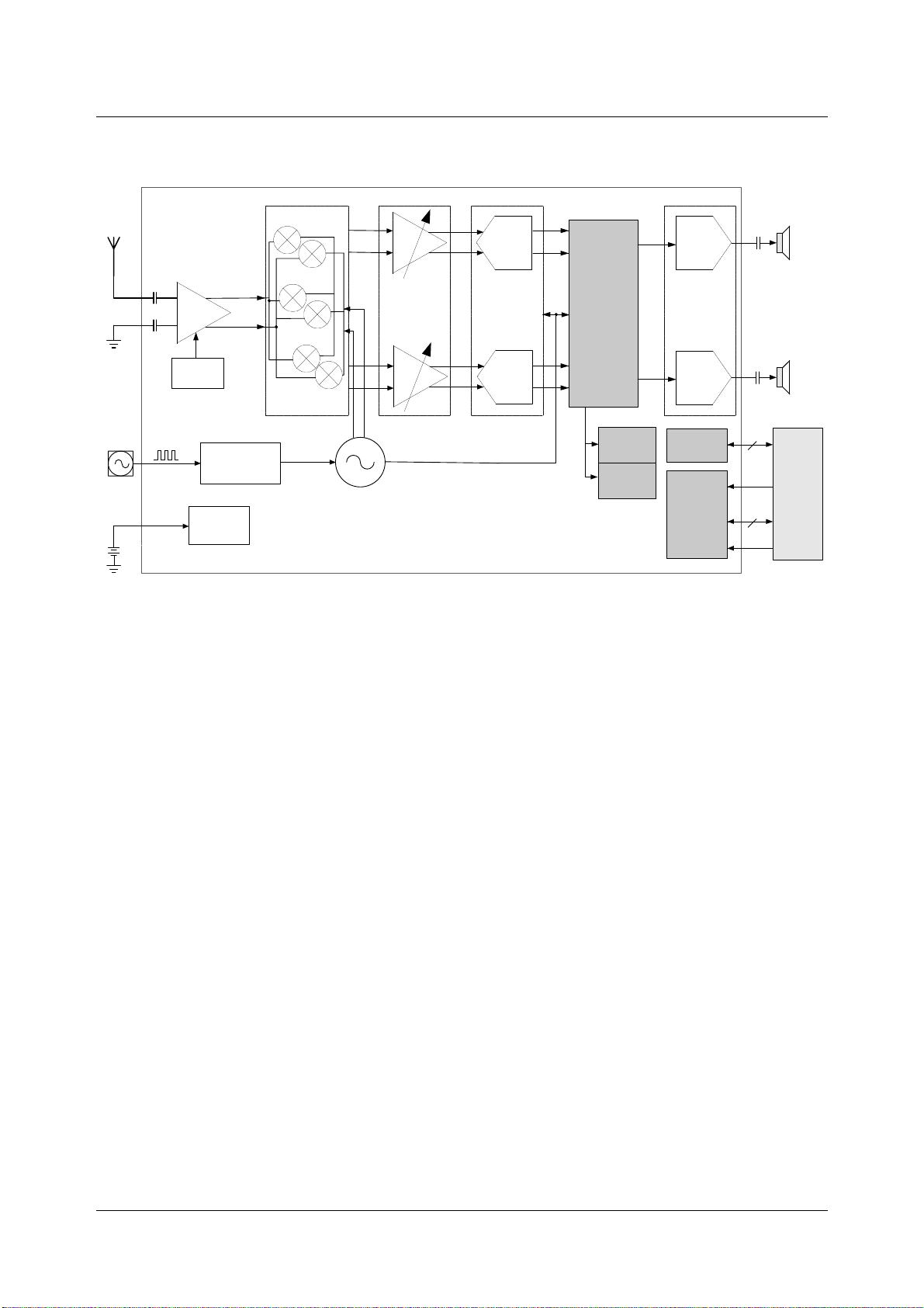
1 General Description
The RDA5802N series is the newest generation
single-chip broadcast FM stereo radio tuner with fully
integrated synthesizer, IF selectivity, RDS/RBDS and
MPX decoder. The tuner uses the CMOS process,
support multi-interface and require the least external
component. The RDA5802N series have three type
package sizes , respective are RDA5802N (QFN 4X4
mm, 24pins), RDA5802NS (QFN 3X3 mm, 20pins) and
RDA5802NM (QFN 2X2 mm, 12pins). All these make it
very suitable for portable devices.
The RDA5802N series has a powerful low-IF digital
audio processor, this make it have optimum sound
quality with varying reception conditions.
The RDA5802N series support frequency range is from
50MHz to 115MHz.
1.1 Features
CMOS single-chip fully-integrated FM tuner
Low power consumption
Total current consumption lower than 20mA at 3.0V
power supply when under normal situation
Support worldwide frequency band
50 -115 MHz
Support flexible channel spacing mode
100KHz, 200KHz, 50KHz and 25KHz
Support RDS/RBDS
Digital low-IF tuner
Image-reject down-converter
High performance A/D converter
IF selectivity performed internally
Fully integrated digital frequency synthesizer
Fully integrated on-chip RF and IF VCO
Fully integrated on-chip loop filter
Autonomous search tuning
Support 32.768KHz crystal oscillator
Digital auto gain control (AGC)
Digital adaptive noise cancellation
Mono/stereo switch
Soft mute
High cut
Programmable de-emphasis (50/75
s)
Receive signal strength indicator (RSSI) and SNR
Bass boost
Volume control and mute
I
2
S digital output interface
Line-level analog output voltage
32.768 KHz 12M,24M,13M,26M,19.2M,38.4MHz
Reference clock
Only support 2-wire bus interface
2
3
4
5
6
1
7
17
16
15
14
13
18
8 9 10 11 12
24 23 22 21 20 19
GND
PAD
GND
GND
LNAP
GND
RDA
5802N
VDD
GND
LOUT
GND
LNAN
ROUT
GND
VDD
GND
GND
SCLK
SDIO
RCLK
VIO
GND
NC
NC
GPIO1
GPIO2
GPIO3
Figure1-1. RDA5802N Top View


剩余28页未读,继续阅读
资源评论

 lixiao_11162016-08-09Hardware-firmware Interface Design
- johnsonsam2014-10-04及时雨啊,客户急着要芯片资料,一时手头又没有,还好在这里找到了。


