P24C64C芯片资料
需积分: 9 35 浏览量
2022-09-19
16:12:57
上传
评论
收藏 404KB PDF 举报


1/21
I
2
C-Compatible Serial E
2
PROM
Data Sheet Rev. 1.2
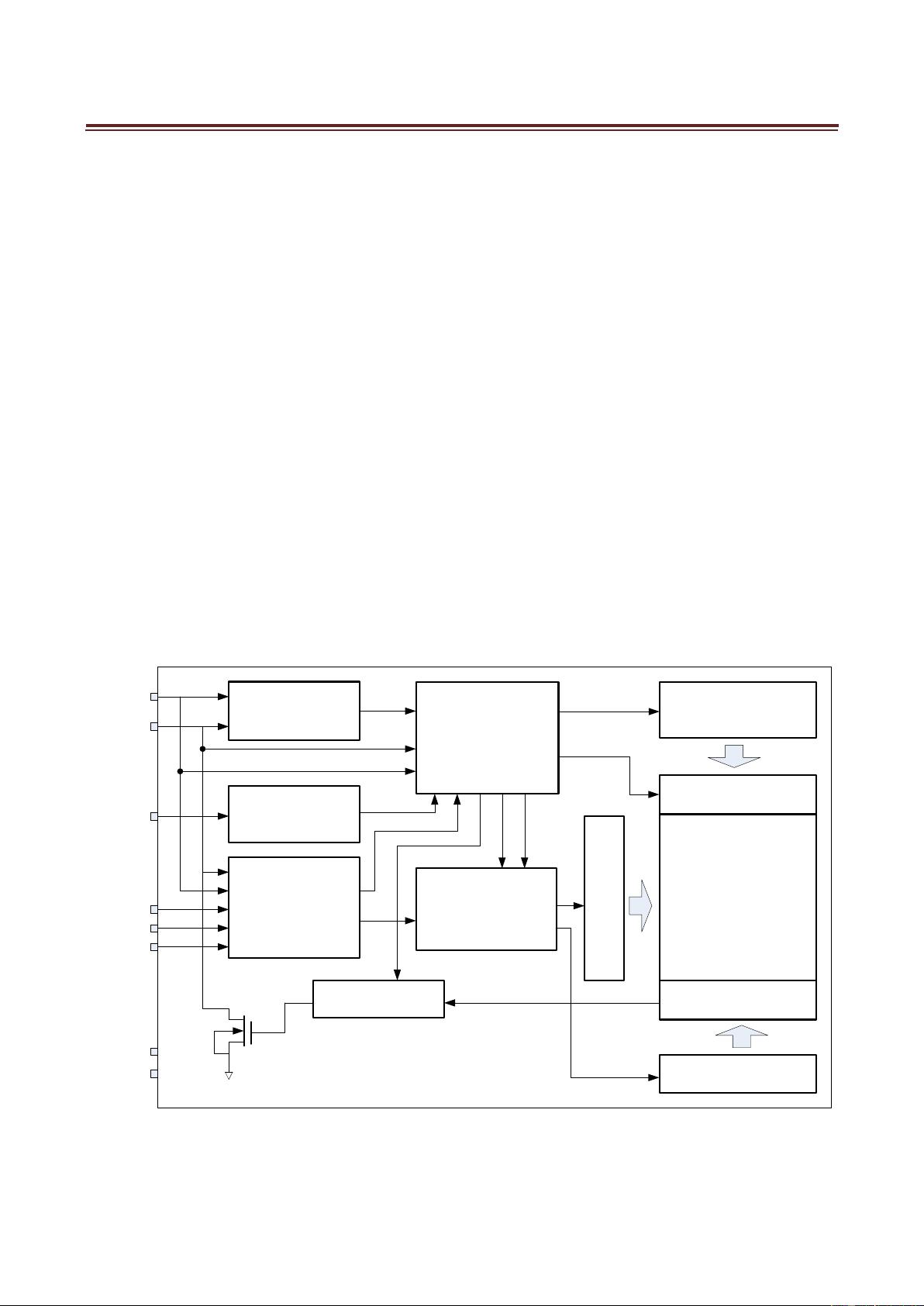
General Description
The P24C64C is a 64-Kbit I
2
C-compatible Serial EEPROM (Electrically Erasable Programmable Memory)
device. It contains a memory array of 8K × 8 bits, which is organized in 32-byte per page.
P24C64C provides the following devices for different application.
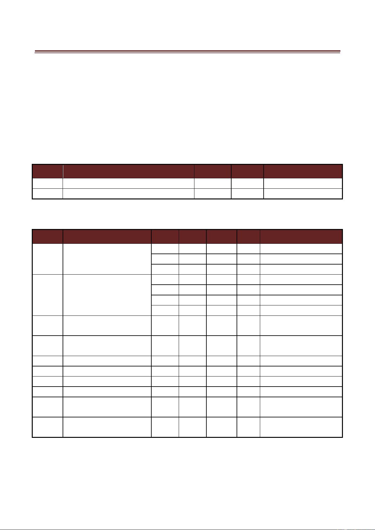
Device Selection Table
Device Name
Voltage Range
Temp. Range
Max. Clock Frequency
P24C64C-MI
1.7V~5.5V
-40°C ~ 85°C
1MHz
[1]
P24C64C-NK
1.8V~5.5V
-40°C ~105°C
1MHz
[1]
P24C64C-DE
2.5V~5.5V
-40°C ~125°C
1MHz
Note 1: 400 kHz for V
CC
< 2.5V.
Features
◼ Single Supply Voltage and High Speed
Minimum operating voltage down to 1.7V
1 MHz clock from 2.5V to 5.5V
400kHz clock from 1.7V to 2.5V
◼ Low power CMOS technology
Read current 400uA, maximum
Write current 1.0mA, maximum
◼ Schmitt Trigger, Filtered Inputs for Noise Suppression
◼ Sequential & Random Read Features
◼ 32 byte Page Write Modes, Partial Page Writes Allowed
◼ Write protect of the whole memory array
◼ Additional Write Lockable Page
◼ Additional 128-bit Serial Number
◼ Self-timed Write Cycle (5ms maximum)
◼ High Reliability
Endurance: 1 Million Write Cycles
Data Retention: 100 Years
HBM: 6KV
Latch up Capability: +/- 200mA (25°C & 125°C )
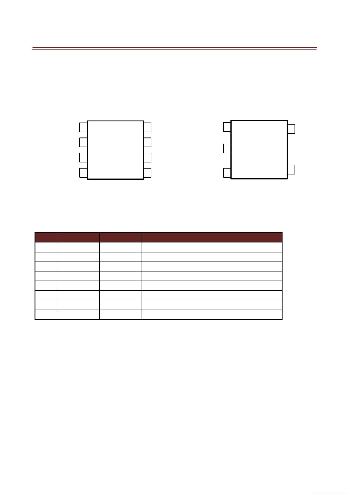
◼ Package: PDIP, SOP, TSSOP, DFN/UDFN and SOT23-5
P24C64C
剩余20页未读,继续阅读
资源评论


