


AN10997
TDA8035 Smart Card Reader
Rev. 1.3 — 4 October 2012
Application note
Document information
Info
Content
Keywords
TDA8035HN, Smart Card Interface, Pay TV, STB, NDS, ISO 7816-3
Abstract This application note describes the smart card interface integrated circuit
TDA8035HN.
This document helps to design the TDA8035HN in an application. The
general characteristics are presented and different application examples
are described.

NXP Semiconductors
AN10997
TDA8035
AN10997
All information provided in this document is subject to legal disclaimers.
© NXP B.V. 2012. All rights reserved.
Application note
Rev. 1.3 — 4 October 2012
2 of 41
Contact information
For additional information, please visit: http://www.nxp.com
For sales office addresses, please send an email to: salesaddresses@nxp.com
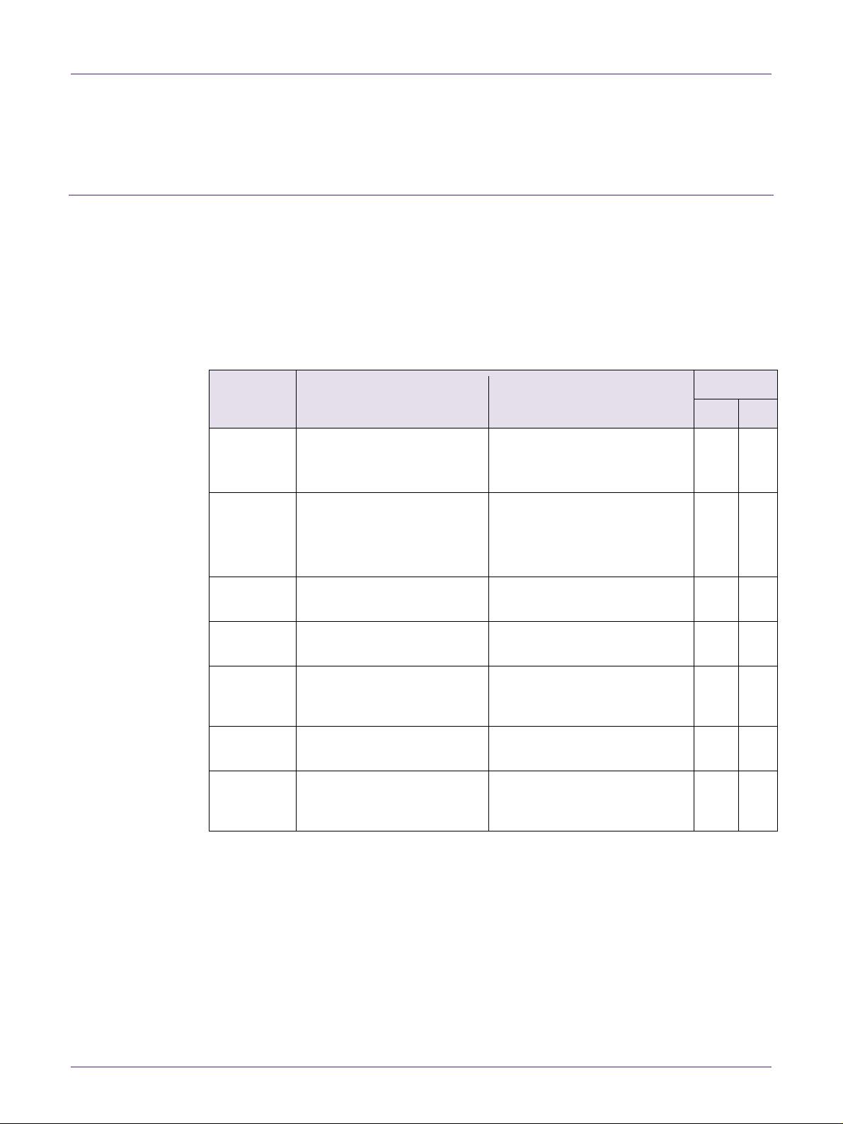
Revision history
Rev
Date
Description
1.3 20121004 Update DC/DC capacitors description
1.2 20120404 Entering test mode description
1.1
20120124
PRESN pull-up resistor calculation added
1.0 20110401 Initial version
NXP Semiconductors
AN10997
TDA8035
AN10997
All information provided in this document is subject to legal disclaimers.
© NXP B.V. 2012. All rights reserved.
Application note
Rev. 1.3 — 4 October 2012
3 of 41
1. Introduction
1.1 Presentation
The TDA8035HN is a smart card interface device forming the electrical interface between
a micro controller and a smart card. This device mainly supports asynchronous cards
(micro controller-based IC cards).
The electrical characteristics of the TDA8035HN are in accordance with NDS
requirements (IRD Electrical Interface Specifications doc n° LC-T056) and also comply
with ISO7816-3 for class A, B and C cards.
The TDA8035HN can be used in various applications such as pay-TV, Point-Of-Sale
terminals (POS), public phones, vending machines, and many conditional access
applications (i.e. Internet,..).
Fig 1. Simplified interfacing view
In the whole document, the TDA8035HN will be referred as TDA8035.
NXP Semiconductors
AN10997
TDA8035
AN10997
All information provided in this document is subject to legal disclaimers.
© NXP B.V. 2012. All rights reserved.
Application note
Rev. 1.3 — 4 October 2012
4 of 41
2. Power supply
2.1 Power supply pins
Two input pins are used to supply the TDA8035: V
DD(INTF)
and V
DDP
. One voltage is
internally generated by the TDA8035 and used for the internal digital part. It is available
on V
REG
pin for external decoupling.
V
DD(INTF)
is dedicated to the interface supply. All signals which are interfaced with the host
are referenced to this voltage supply.
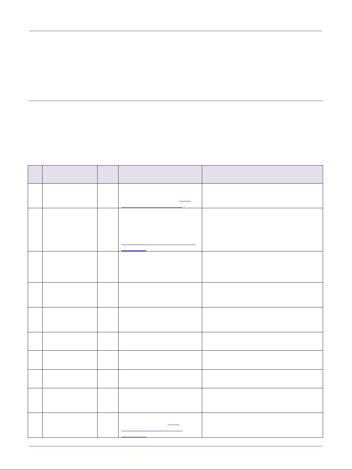
The next table describes all the pins that must be referenced to V
DD(INTF).
Table 1. V
DD(INTF)
referenced pins
Pin name Comment
IOUC Smart card data. Controlled by the microcontroller
PORADJ External configuration of V
DD(INTF)
supervision threshold
CMDVCCN Smart card activation. Controlled by a microcontroller
GPIO
CLKDIV1
Control of the clock division. Can be controlled by the
microcontroller or connected directly to GND or V
DD(INTF)
CLKDIV2 Control of the clock division. Can be controlled by the
microcontroller or connected directly to GND or V
DD(INTF)
EN5V_3VN Choice of the smart card voltage. Can be controlled by
the microcontroller or connected directly to GND or
V
DD(INTF)
EN1.8VN Choice of the 1.8V smart card voltage. Can be controlled
by the microcontroller or connected directly to GND or
V
DD(INTF)
RSTIN RST pin management. Controlled by a microcontroller
GPIO
OFFN Output to the host. Must be connected to the
microcontroller and therefore have the same level
XTAL1 External oscillator, or crystal input
XTAL2 Crystal output
CS
Chip select signal
PRESN
Not connected to the microcontroller but reference to
V
DD(INTF)
. The smart card connector presence switch must
use V
DD(INTF)
AUX1UC Management of AUX1. Controlled by the microcontroller
AUX2UC Management of AUX2. Controlled by the microcontroller
NXP Semiconductors
AN10997
TDA8035
AN10997
All information provided in this document is subject to legal disclaimers.
© NXP B.V. 2012. All rights reserved.
Application note
Rev. 1.3 — 4 October 2012
5 of 41
V
DDP
is used to supply the DC/DC converter of the TDA8035 and the internal regulator
used to generate V
REG
.
V
REG
supplies the core of the TDA8035. It is generated by the TDA8035. Its value is
always 1.8 V.
2.2 Supply supervisor
2.2.1 Main principles
The TDA8035 supervises the voltage level of V
REG
, V
DDP
and V
DD(INTF)
. For V
REG
and V
DDP
supervision, the threshold is internally fixed. For V
DD(INTF)
, the threshold can be fixed
either internally or externally using the PORAdj pin.
The following figure explains the supervision for all the supplies.
Then the table gives the threshold values for each input.
(1) When one power supply input falls below its corresponding threshold, the TDA8035 is in reset
mode. When all the levels are above their threshold + the hysteresis, the TDA8035 is ON.
Fig 2. Supply supervisor principles


- 1
- 2
- 3
前往页