Rev. A 09/12
3
TNY284-290
www.powerint.com
to provide an output overvoltage function with a Zener
connected from the BYPASS/MULTI-FUNCTIONAL pin to a
bias winding supply.
ENABLE/UNDERVOLTAGE (EN/UV) Pin:
This pin has dual functions: enable input and line undervoltage
sense. During normal operation, switching of the power
MOSFET is controlled by this pin. MOSFET switching is
terminated when a current greater than a threshold current is
drawn from this pin. Switching resumes when the current being
pulled from the pin drops to less than a threshold current. A
modulation of the threshold current reduces group pulsing. The
threshold current is between 75 μA and 115 μA.
The ENABLE/UNDERVOLTAGE pin also senses line
undervoltage conditions through an external resistor connected
to the DC line voltage. If there is no external resistor connected
to this pin, TinySwitch-4 detects its absence and disables the
line undervoltage function.
SOURCE (S) Pin:
This pin is internally connected to the output MOSFET source
for high-voltage power return and control circuit common.
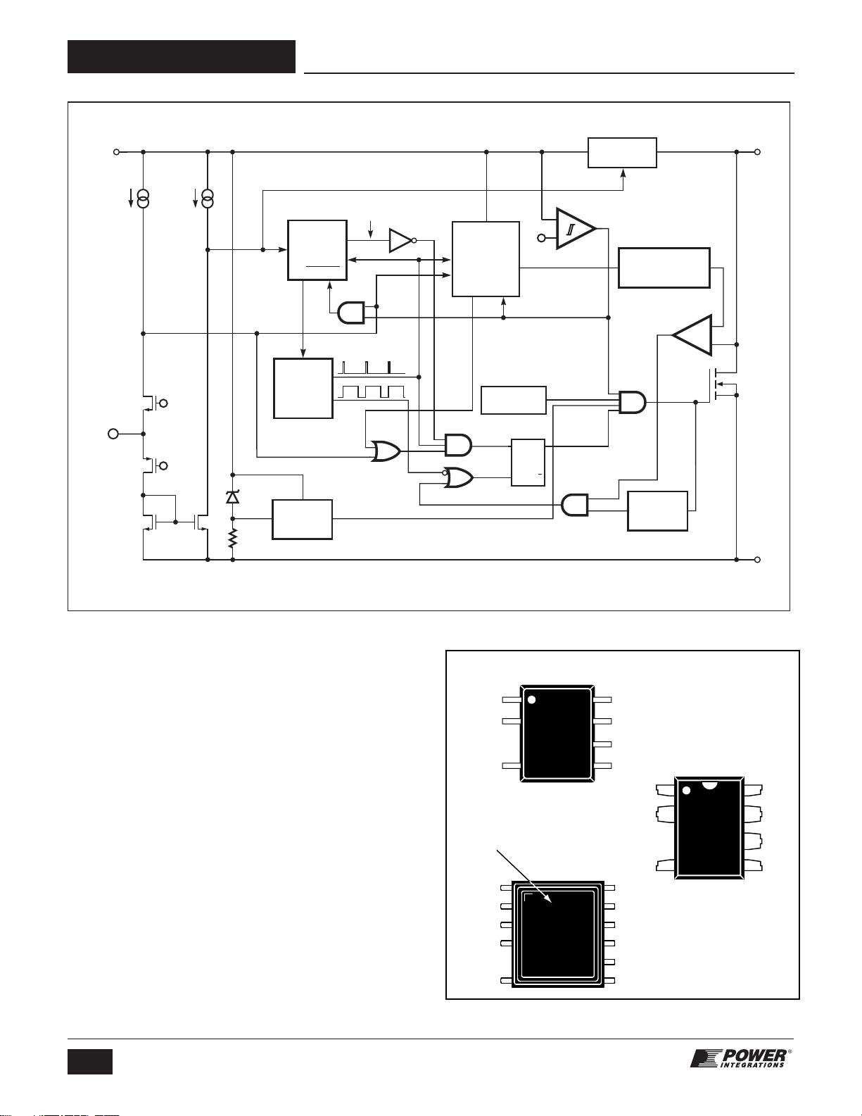
TinySwitch-4 Functional Description
TinySwitch-4 combines a high-voltage power MOSFET switch
with a power supply controller in one device. Unlike conventional
PWM (pulse width modulator) controllers, it uses a simple
ON/OFF control to regulate the output voltage.
The controller consists of an oscillator, enable circuit (sense and
logic), current limit state machine, 5.85 V regulator, BYPASS/
MULTI-FUNCTION pin undervoltage, overvoltage circuit, and
current limit selection circuitry, over-temperature protection,
current limit circuit, leading edge blanking, and a 725 V power
MOSFET. TinySwitch-4 incorporates additional circuitry for line
undervoltage sense, auto-restart, adaptive switching cycle
on-time extension, and frequency jitter. Figure 3 shows the
functional block diagram with the most important features.
Figure 5. Frequency Jitter.
0510
136 kHz
128 kHz
V
DRAIN
Time (µs)
PI-2741-041901
500
400
300
200
100
0
Oscillator
The typical oscillator frequency is internally set to an average of
132 kHz. Two signals are generated from the oscillator: the
maximum duty cycle signal (DC
MAX
) and the clock signal that
indicates the beginning of each cycle.
The oscillator incorporates circuitry that introduces a small
amount of frequency jitter, typically 8 kHz peak-to-peak, to
minimize EMI emission. The modulation rate of the frequency
jitter is set to 1 kHz to optimize EMI reduction for both average
and quasi-peak emissions. The frequency jitter should be
measured with the oscilloscope triggered at the falling edge of
the DRAIN waveform. The waveform in Figure 5 illustrates the
frequency jitter.
Enable Input and Current Limit State Machine
The enable input circuit at the ENABLE/UNDERVOLTAGE pin
consists of a low impedance source follower output set at 1.2 V.
The current through the source follower is limited to 115 μA.
When the current out of this pin exceeds the threshold current,
a low logic level (disable) is generated at the output of the
enable circuit, until the current out of this pin is reduced to less
than the threshold current. This enable circuit output is
sampled at the beginning of each cycle on the rising edge of the
clock signal. If high, the power MOSFET is turned on for that
cycle (enabled). If low, the power MOSFET remains off
(disabled). Since the sampling is done only at the beginning of
each cycle, subsequent changes in the ENABLE/UNDER-
VOLTAGE pin voltage or current during the remainder of the
cycle are ignored.
The current limit state machine reduces the current limit by
discrete amounts at light loads when TinySwitch-4 is likely to
switch in the audible frequency range. The lower current limit
raises the effective switching frequency above the audio range
and reduces the transformer flux density, including the
associated audible noise. The state machine monitors the
sequence of enable events to determine the load condition and
adjusts the current limit level accordingly in discrete amounts.
Under most operating conditions (except when close to
no-load), the low impedance of the source follower keeps the
voltage on the ENABLE/UNDERVOLTAGE pin from going much
below 1.2 V in the disabled state. This improves the response
time of the optocoupler that is usually connected to this pin.
5.85 V Regulator and 6.4 V Shunt Voltage Clamp
The 5.85 V regulator charges the bypass capacitor connected
to the BYPASS pin to 5.85 V by drawing a current from the
voltage on the DRAIN pin whenever the MOSFET is off. The
BYPASS/MULTI-FUNCTION pin is the internal supply voltage
node. When the MOSFET is on, the device operates from the
energy stored in the bypass capacitor. Extremely low power
consumption of the internal circuitry allows TinySwitch-4 to
operate continuously from current it takes from the DRAIN pin.
A bypass capacitor value of 0.1 μF is sufficient for both high
frequency decoupling and energy storage.
In addition, there is a 6.4 V shunt regulator clamping the
BYPASS/MULTI-FUNCTION pin at 6.4 V when current is
provided to the BYPASS/MULTI-FUNCTION pin through an


 我的内容管理
展开
 我的资源
快来上传第一个资源
 我的收益 登录查看自己的收益
 我的积分
登录查看自己的积分
 我的C币
登录后查看C币余额
 我的收藏
我的收藏  我的下载
我的下载  下载帮助
下载帮助 
 前往需求广场,查看用户热搜

 信息提交成功