UHD-SDI Gearbox
需积分: 15 161 浏览量
2016-04-14
15:50:24
上传
评论
收藏 1.84MB PDF 举报

1 of 45
Semtech
Proprietary & Confidential
GS12070
Draft Data Sheet Rev.2
PDS-061012 October 2015
GS12070
UHD-SDI Gearbox
www.semtech.com
Key Features
• Converts between HD-SDI, 3G-SDI, 6G UHD-SDI, and
12G UHD-SDI using MUX (Multiplex) and DeMUX
(Demultiplex) modes
Quad Link 3G-SDI ↔ Single Link 12G UHD-SDI
Dual Link 6G UHD-SDI ↔ Single Link 12G UHD-SDI
Dual Link 3G-SDI (ST 425-3) ↔ Single Link 6G
UHD-SDI
Quad Link 3G-SDI (ST 425-5/6) ↔ Dual Link 6G
UHD-SDI
Quad Link (1.5Gb/s x 4) HD-SDI ↔ Single Link 6Gb/s
Dual Link (1.5Gb/s x 2) HD-SDI ↔ Single Link 3Gb/s
• Bypass modes for all support rates
• Configurable Serial Output reassignment
• Four 100Ω Differential Inputs
Individually selectable input trace equalization for
up to 12dB boost
• Four 100Ω Differential Outputs
Individually selectable output swing and
de-emphasis
• Reference Clock/Crystal Input — 27MHz
Optional support 148.5MHz reference
• GSPI Serial Control and monitoring Interface
• Automatic SMPTE ST 352 packet creation
• Receiver H Sync Outputs per Lane
• 12mm x 12mm 196-Ball BGA (0.8mm pitch)
• Pb-free and RoHS-compliant package
Applications
Next Generation 3D/2D HFR HDTV and 2K D-Cinema,
UHDTV1 and 4K D-Cinema end-equipment: Cameras,
Monitors, Switchers, etc.
Next Generation 3G-SDI, 6G UHD-SDI, and 12G UHD-SDI
infrastructures designed in support of UHDTV1, UHDTV2,
4K D-Cinema and 3D HFR, HDR production image formats,
and 6G UHD-SDI/12G UHD-SDI multiplexing and
de-multiplexing for integration into legacy infrastructure.
Description
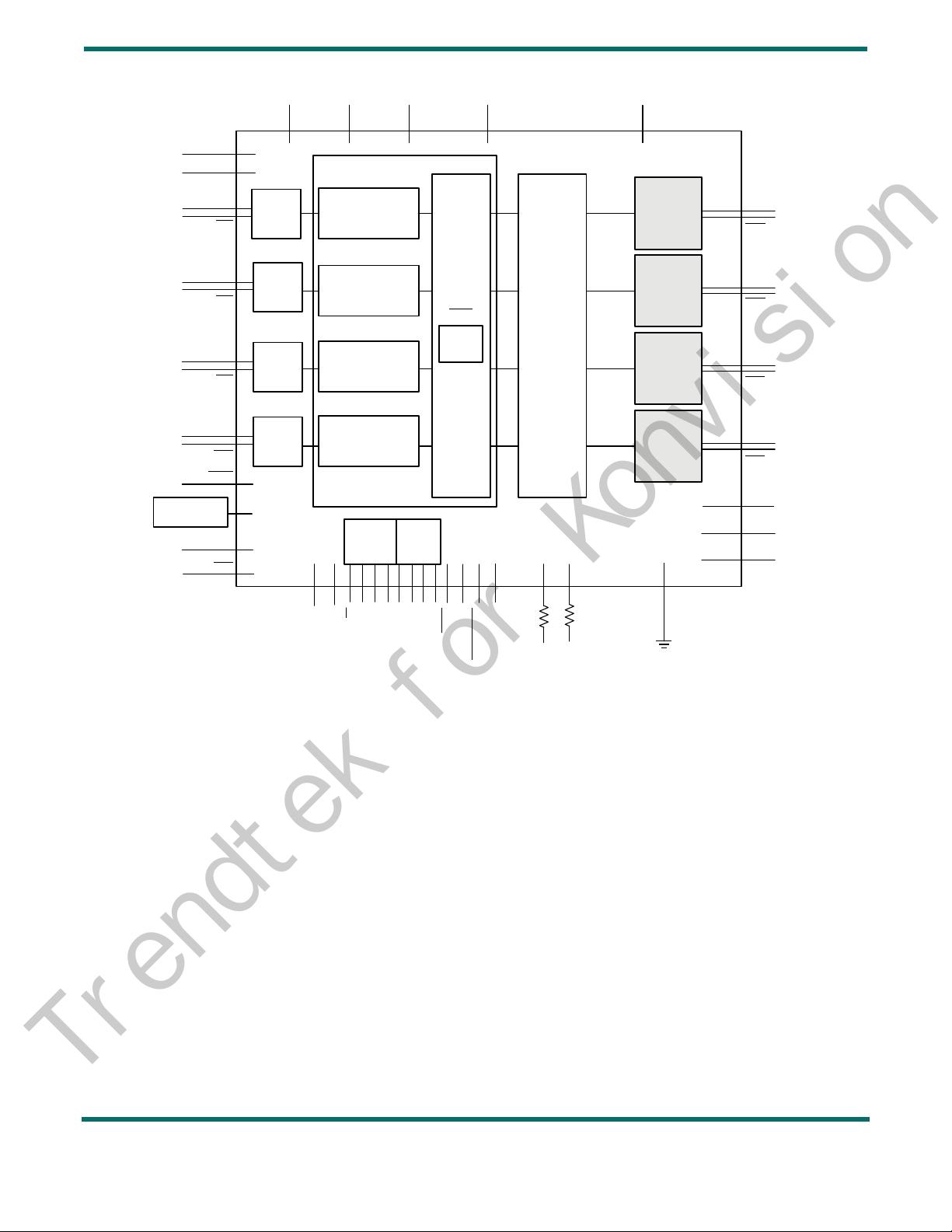
The GS12070 is highly configurable UHD-SDI Gearbox
which performs multiplexing and de-multiplexing
necessary to facilitate conversions between SMPTE ST
425-3 and/or ST 425-5 (multi-link 3G-SDI) Interface and
SMPTE ST 2081-1 (6G UHD-SDI) and/or ST 2082-1 (12G
UHD-SDI) Interfaces. The Gearbox also supports conversion
between 4 x HD-SDI and 6Gb/s SDI.
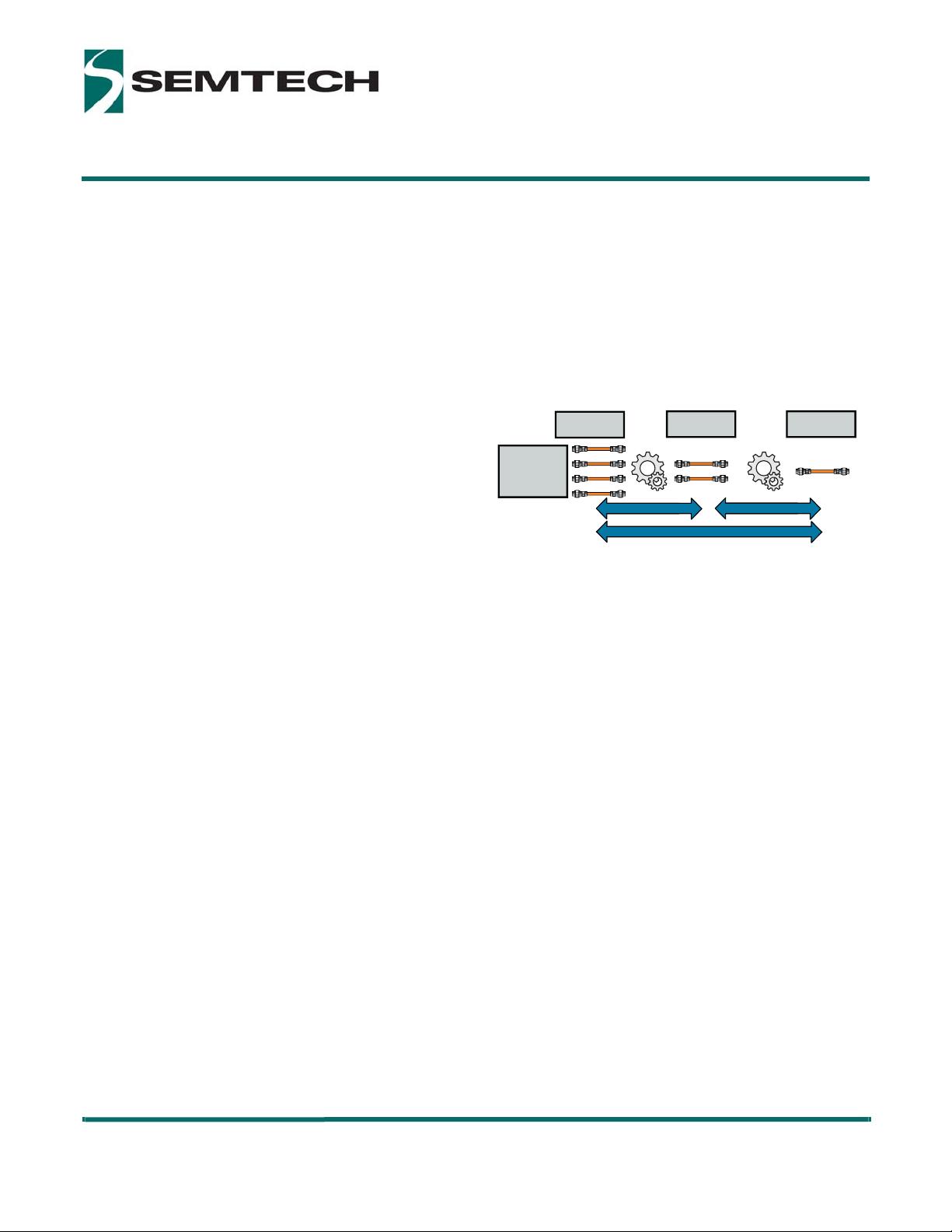
Example of Multiplexing ST 525-5 into ST 2081-1 (6Gb/s) and
ST 2082-1 (12Gb/s)
For the supported SMPTE conversions, the SMPTE ST 352
payload identification will be automatically detected and
replaced based on the user selected conversion mode. This
can be bypassed for proprietary multiplexing and
demultiplexing links.
The device incorporates the ability to reorder the output
serial stream and duplicate outputs to unused output
channels or route any input channel.
The GS12070 features four high-speed differential signal
inputs and four high-speed differential serial outputs of up
to 11.88Gb/s. The high-speed inputs and outputs include
programmable trace equalization and de-emphasis drivers
to compensate for high-frequency losses associated with
board-level interconnectivity.
The GS12070 has the ability to automatically compensate
for up to 400ns of skew mismatch on a QL 6Gb/s or DL
12Gb/s and 800ns of skew mismatch on a DL 6Gb/s and QL
3Gb/s. This aids in any lane-to-lane variance introduced by
cable mismatch or upstream routing and distribution
equipment.
In DeMUX mode to quad 3G the outputs can be manually
delayed for up to 6.8μs in 6.7ns increments.
3840 x 2160
p60
4:2:2 10-bit
ST 425-5
Quad-link 3G
ST 2081-11
Dual-link 6G
ST 2082-10
Single-link 12G
4 x 3G ↔ 12G
4 x 3G ↔ 2 x 6G
2 x 6G ↔ 12G


剩余44页未读,继续阅读
资源评论


iyandy
- 粉丝: 4
- 资源: 15


