没有合适的资源?快使用搜索试试~ 我知道了~
资源推荐
资源详情
资源评论
V
V
e
e
r
r
i
i
S
S
i
i
l
l
i
i
c
c
o
o
n
n
S
S
M
M
I
I
C
C
0
0
.
.
1
1
8
8
µ
µ
m
m
1
1
.
.
8
8
V
V
/
/
3
3
.
.
3
3
V
V
I
I
/
/
O
O
C
C
e
e
l
l
l
l
L
L
i
i
b
b
r
r
a
a
r
r
y
y
D
D
a
a
t
t
a
a
b
b
o
o
o
o
k
k
Version: 2.0
July 1, 2003
Trademark Acknowledgments
VeriSilicon & the VeriSilicon logo are the trademarks of VeriSilicon Microelectronics
(Shanghai) Co., Ltd.
All other products and company names mentioned may be the trademarks of their
respective owners.
© 2002 VeriSilicon Microelectronics (Shanghai) Co., Ltd. All rights reserved.
Printed in P.R.China.
VeriSilicon Microelectronics (Shanghai) Co., Ltd. reserves all its
copy rights and other intellectual property rights, ownership,
powers, benefits and rights arising or to arise from this manual.
All or part of the contents of this manual may be changed by
VeriSilicon Microelectronics (Shanghai) Co., Ltd. without notice
at any time for any reason, including but not limited to
improvement of the product relating hereto.
VeriSilicon Microelectronics (Shanghai) Co., Ltd. shall not
undertake or assume any obligation, responsibility or liability
arising out of or in respect of the application or use of the
product described herein, except for reasonable, careful and
normal uses.
Nothing, whether in whole or in part, within this manual can be
reproduced, duplicated, copied, changed or disposed of in any
form or by any means without prior written consent by
VeriSilicon Microelectronics (Shanghai) Co., Ltd..
VeriSilicon Microelectronics (Shanghai) Co., Ltd.
3F, Building 1, No.200, Zhangheng Road, Zhangjiang Hi-Tech Park, Pudong
New Area, Shanghai 201204, P. R. China
Tel : +86-21-5131-1118
Fax : +86-21-5131-1119
Web : http://www.verisilicon.com
3
Contents
Library Introduction 4
1.1 Library Description ....................................................4
1.2 Geometry Parameters...............................................4
1.3 Operating Conditions ................................................4
1.4 DC Specifications .....................................................4
1.5 Timing Parameters....................................................5
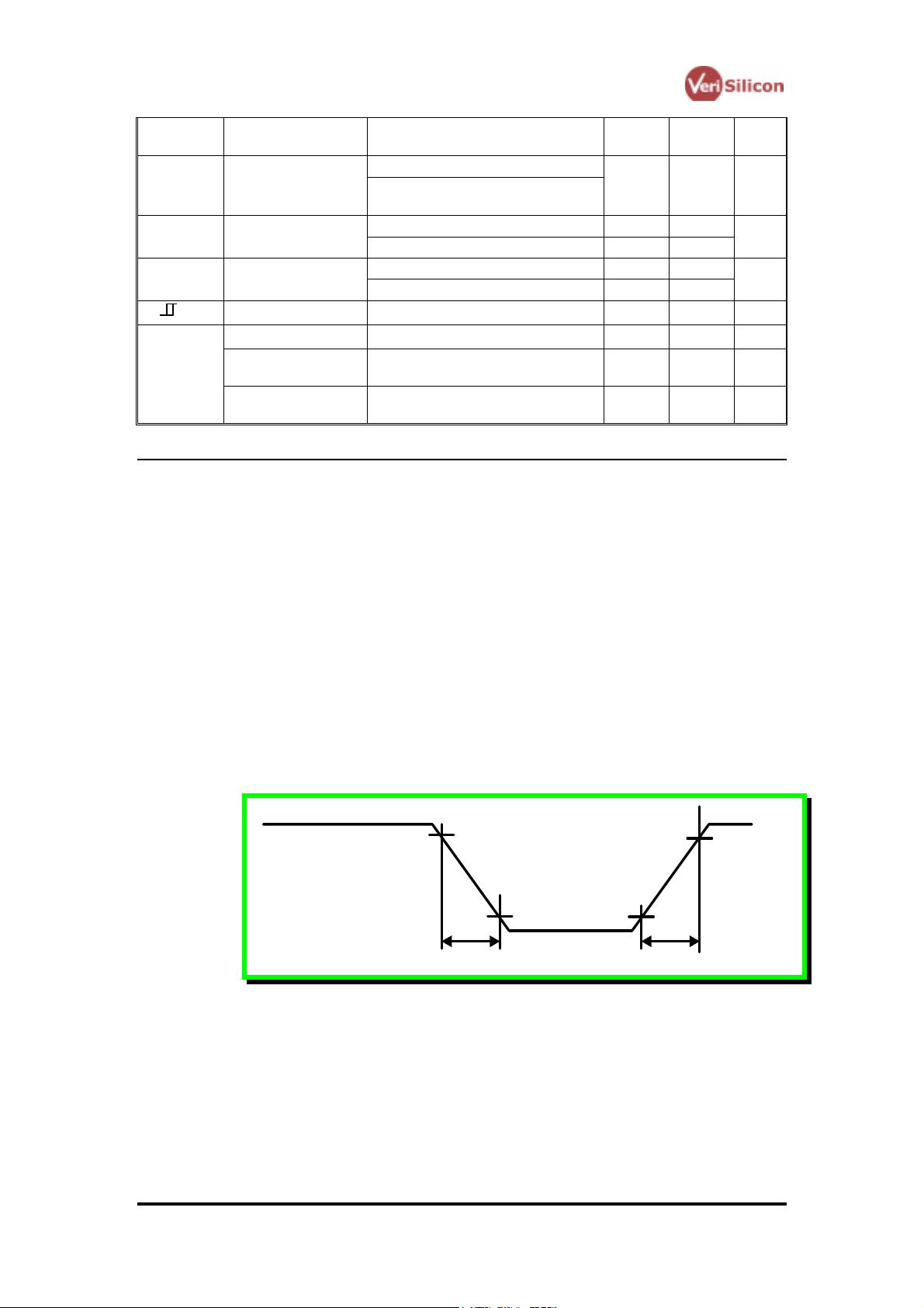
Rise/Fall Transition Time ------------------------------5
Propagation Delay---------------------------------------5
1.6 Power Characterization.............................................6
Power Dissipation----------------------------------------6
Dynamic Power Dissipation ---------------------------6
Static Power Dissipation -------------------------------6
Power Dissipation Calculation------------------------6
Power Characterization Example--------------------7
1.7 Derating Factors .......................................................8
Delay Calculation ----------------------------------------8
Cell Naming Conventions 9
2.1 Naming Conventions.................................................9
I/O Cell Descriptions 11
3.1 Cell Type.................................................................11
3.2 Pin Descriptions for I/O Pads..................................11
Input-Output Pads ------------------------------------- 11
Oscillator Pads ----------------------------------------- 11
Analog I/O Pads---------------------------------------- 12
Power/Ground Pads----------------------------------- 12
3.3 Functional Schematic for I/O Pads..........................13
Input-Output Pads ------------------------------------- 13
Oscillator Pads ----------------------------------------- 13
3.4 Truth Table of I/O Pads...........................................14
Description----------------------------------------------- 14
Configuration Table ----------------------------------- 14
3.5 I/O Cell List .............................................................33
I/O Cell Datasheet 36
4.1 I/O Cell Height and Width .......................................36
4.2 Explanation of the Cell Datasheet...........................38
4.3 Datasheet ...............................................................39
VeriSilicon SMIC 0.18um 1.8V/3.3V I/O Cell Library Databook Library Introduction
4
chapter 1
Library Introduction
1.1 Library Description
VeriSilicon SMIC 0.18µm 1.8V/3.3V I/O Cell Library developed by
VeriSilicon is optimized for Semiconductor Manufacturing International
Corporation (SMIC) 0.18µm Logic 1P6M Salicide 1.8/3.3V process. This
library supports both Stagger I/O pads and Inline I/O pads. This library can
take 5V tolerance configurable and variable driving strength between 2mA
- 24mA.
1.2 Geometry Parameters
VeriSilicon SMIC 0.18µm 1.8V/3.3V I/O Cell Library supports design with
four, five or six layers of metal.
1.3 Operating Conditions
The following table gives the recommended operating conditions for the
integrated circuits (IC) chips using this library:
Recommended Operating Conditions
Operating Conditions Typical Minimum Maximum
Core DC Supply Voltage
1.8V 1.62V 1.98V
I/O DC Supply Voltage
3.3V 3.0V 3.6V
Junction Temperature
25°C 0°C 125°C
1.4 DC Specifications
The ESD of VeriSilicon SMIC 0.18(m 1.8V/3.3V I/O Cell Library meets
HBM-2KV and MM-200V.
The following table summarizes the electrical design specifications of DC
specifications:
DC Specifications
Symbol Parameter Condition Min Max Unit
VOH
High level output
IOH = -2, -4, -8, -16, -24mA 2.4 V
VeriSilicon SMIC 0.18um 1.8V/3.3V I/O Cell Library Databook Library Introduction
5
voltage
Programmable type: -24mA ≤ I
OH
≤
-2mA
I
OL =
2, 4, 8, 16, 24mA
V
OL
Low level output
voltage
Programmable type: 2mA ≤ I
OH
≤
24mA
0.4 V
CMOS interface 2.0
V
IH
High level input
voltage
CMOS Schmitt trigger interface 1.4 2.0
V
CMOS interface 0.8
V
IL
Low level input
voltage
CMOS Schmitt trigger interface 0.8 1.2
V
Hysteresis
0.6 0.9 V
Input current
Vdd = MAX, 0V ≤ Vin ≤ 5.5V
-10 10
µA
Input current with
40kΩ pull down
Vin = Vdd 40 160
µA
I
I
Input current with
40kΩ pull up
Vin = 0 -160 40
µA
1.5 Timing Parameters
The following timing parameters are used in cell characterization.
Rise/Fall Transition Time
One of the most important timing parameters used in cell characterization
is the transition time. The rise time is the minimum time required for the
output signal transits from logic 0 to logic 1; more precisely, it is the time
from the point where the output transition reaches 10% of the supply
voltage to the point where the output transition reaches 90% of the supply
voltage; The fall time is the minimum time required for the output signal
transits from logic 1 to logic 0; more precisely, it is the time from the point
where the output transition reaches 90% of the supply voltage to the point
where the output transition reaches 10% of the supply voltage (Fig. 1).
tf
90% Vdd
10% Vdd
90% Vdd
10% Vdd
tr
Fig. 1 Rise/Fall Transition Time
Propagation Delay
The propagation delay is the minimum time required for data to be
propagated from the input of the cell to the output; more precisely, it is the
time from the point where the input transition reaches 50% of the supply
voltage to the point where the output transition reaches 50% of the supply
voltage (Fig. 2).
VeriSilicon SMIC 0.18um 1.8V/3.3V I/O Cell Library Databook Library Introduction
剩余522页未读,继续阅读
资源评论
- zlb212013-10-31这个我还是看不懂,而且不能用于DC
- XIDIANZHANGJIANING2012-06-02这个我还是看不懂,而且不能用于DC
- tyjujjqaz2013-11-14没看懂~本来想下库文件,结果下成这个了。。。。
huozhu333
- 粉丝: 0
- 资源: 3
上传资源 快速赚钱
- 我的内容管理 展开
- 我的资源 快来上传第一个资源
- 我的收益 登录查看自己的收益
- 我的积分 登录查看自己的积分
- 我的C币 登录后查看C币余额
- 我的收藏
- 我的下载
- 下载帮助
安全验证
文档复制为VIP权益,开通VIP直接复制
信息提交成功