没有合适的资源?快使用搜索试试~ 我知道了~
超结MOS,Rds<=17毫欧
0 下载量 146 浏览量
2022-12-11
22:21:58
上传
评论
收藏 1.39MB PDF 举报
温馨提示
试读
14页
国产超结MOS,品牌:尚阳通; Vds = 600V,Rds 17毫欧,自身内阻是非小,适用于电源LLC等类产品应用。
资源推荐
资源详情
资源评论
Datasheet
17mΩ, 600V, Super Junction N-Channel Power MOSFET SRC60R017FB
Nov. 2022, Rev.1.2 www.sanrise-tech.com Shenzhen Sanrise Technology Co., LTD.
General Description
The Sanrise SRC60R017FB is a high voltage
power MOSFET, fabricated using advanced super
junction technology. The resulting device has
extremely low on resistance, low gate charge and
fast switching time, making it especially suitable
for applications which require superior power
density and outstanding efficiency.
The SRC60R017FB break down voltage is 600V
and it has a high rugged avalanche characteristics.
The SRC60R017FB is available in TO-247
package.
Features
Ultra Low R
DS(ON)
= 17mΩ @ V
GS
= 10V.
Ultra Low Gate Charge, Qg=291nC typ.
Fast switching capability
Robust design with better EAS performance
EMI Improved
Non-automotive Qualified
Ultra-fast body diode
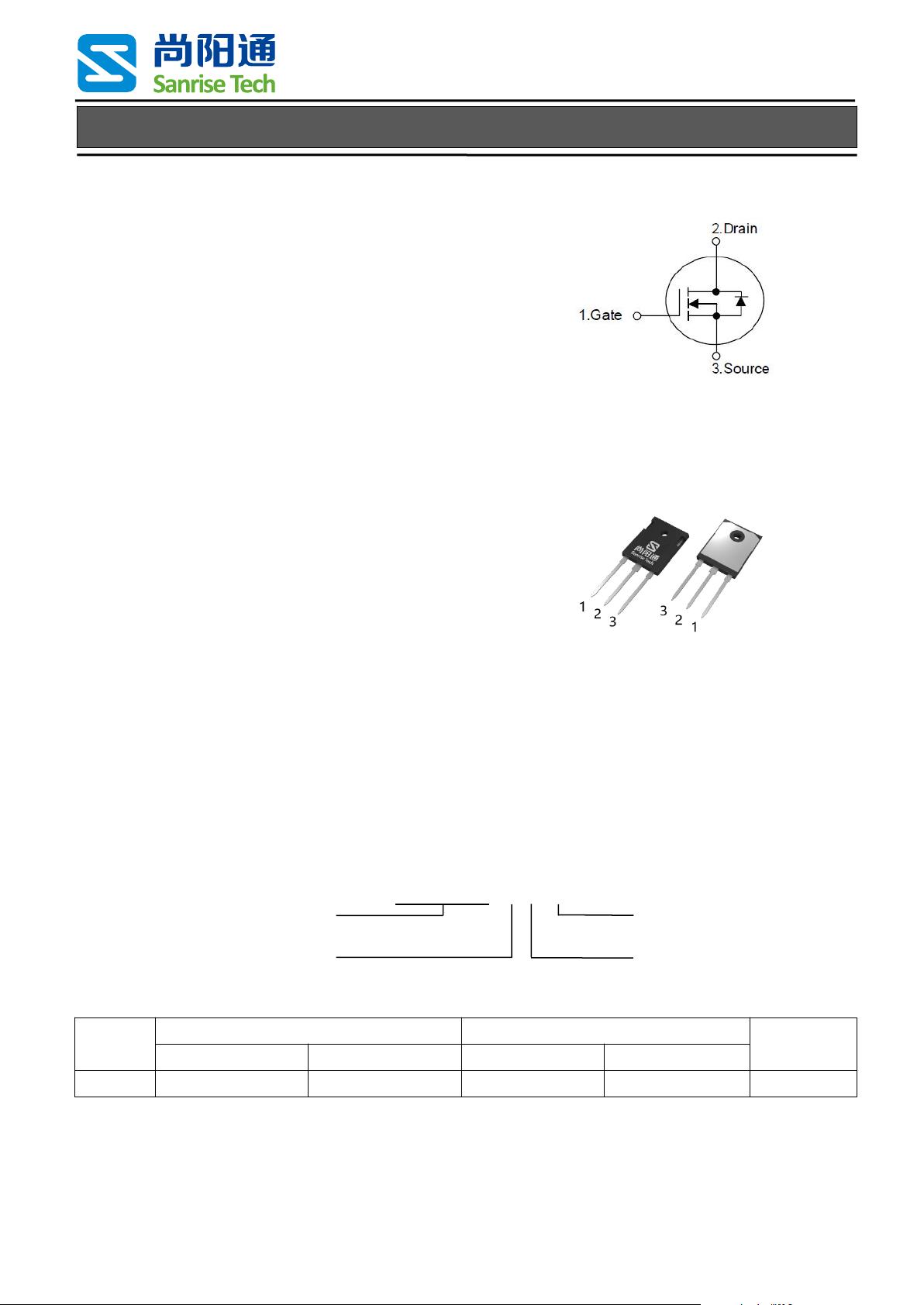
Symbol
Figure 1 Symbol of SRC60R017FB
Package Type
TO-247
Figure 2 Package Type of SRC60R017FB
Application
Sever / Telecom Power
EV Charger
Ordering Information
SRC60R017FB□□–□
Circuit Type E: Lead Free
G: Green
Package Blank: Tube
T: TO-247 TR: Tape & Reel
Package
Part Number
Marking ID
Packing Type
Lead Free
Green
Lead Free
Green
TO-247
SRC60R017FBT-E
SRC60R017FBT-G
SRC60R017FBTE
SRC60R017FBTG
Tube
Datasheet
17mΩ, 600V, Super Junction N-Channel Power MOSFET SRC60R017FB
Nov. 2022, Rev.1.2 www.sanrise-tech.com Shenzhen Sanrise Technology Co., LTD.
Absolute Maximum Ratings
Parameter
Symbol
Rating
Unit
Drain-Source Voltage
V
DSS
600
V
Gate-Source Voltage (static)
V
GSS
±20
V
Gate-Source Voltage (dynamic), AC f>1Hz
V
GSS
±30
V
Power Dissipation(Tc=25℃,TO-247)
P
tot
657
W
Continuous Drain Current
T
C
=25ºC
I
D
120
A
T
C
=100ºC
76
T
C
=125ºC
54
Pulsed Drain Current (Note 2)
I
DM
360
A
Avalanche Energy, Single Pulse (Note 3)
E
AS
600
mJ
Avalanche Energy, Repetitive (Note 2)
E
AR
0.6
mJ
Avalanche Current, Repetitive (Note 2)
I
AR
5.5
A
Continuous Diode Forward Current
I
S
120
A
Diode Pulse Current
I
S.PULSE
360
A
MOSFET dv/dt Ruggedness, V
DS
<=480V
dv/dt
80
V/ns
Reverse Diode dv/dt, V
DS
<=480V, I
SD
<=I
D
dv/dt
50
V/ns
Operating Junction Temperature
T
J
150
ºC
Storage Temperature
T
STG
-55 to 150
ºC
Lead Temperature (Soldering, 10 sec)
T
LEAD
260
ºC
Note:
1. Absolute maximum ratings are those values beyond which the device could be permanently damaged.
Absolute maximum ratings are stress ratings only and functional device operation is not implied.
2. Repetitive Rating: Pulse width limited by maximum junction temperature
3. I
AS
= 5.5A, V
DD
= 60V, R
G
= 25Ω, Starting T
J
= 25°C
Thermal characteristics
Parameter
Symbol
Min
Typ
Max
Unit
Thermal resistance, Junction-to-Case
TO-247
R
thJC
0.19
ºC /W
Thermal resistance, Junction-to-Ambient
TO-247
R
thJA
62
ºC /W
Datasheet
17mΩ, 600V, Super Junction N-Channel Power MOSFET SRC60R017FB
Nov. 2022, Rev.1.2 www.sanrise-tech.com Shenzhen Sanrise Technology Co., LTD.
Electrical Characteristics
T
J
= 25℃, unless otherwise specified.
Parameter
Symbol
Test Conditions
Min
Typ
Max
Unit
Statistic Characteristics
Drain-Source Breakdown Voltage
BV
DSS
V
GS
=0V, I
D
=250uA
600
V
Zero Gate Voltage Drain Current
I
DSS
V
DS
=600V, V
GS
=0V
10
uA
Gate-Body Leakage Current
Forward
I
GSSF
V
GS
=30V, V
DS
=0V
200
nA
Reverse
I
GSSR
V
GS
=-30V, V
DS
=0V
-200
Gate Threshold Voltage
V
GS(TH)
V
DS
=V
GS
, I
D
=2.9mA
3.0
4.0
5.0
V
Static Drain-Source On-Resistance
R
DS(ON)
V
GS
=10V, I
D
=40A
15.1
17
mΩ
Gate Resistance
R
G
f=1MHz, Open Drain
1.3
Ω
Dynamic Characteristics
Input Capacitance
C
ISS
V
DS
=400V, V
GS
=0V,
f=100KHz
13.7
nF
Output Capacitance
C
OSS
222
pF
Effective output capacitance, energy
related
NOTE5
C
O(er)
V
GS
=0V,
V
DS
=0…480V
291
pF
Effective output capacitance, time
related
NOTE6
C
O(tr)
237
9
Turn-on Delay Time
t
d(on)
V
DD
=400V, I
D
=60A
R
G
=2Ω, V
GS
=12V
73.2
ns
Rise Time
t
r
21.6
Turn-off Delay Time
t
d(off)
184
Fall Time
t
f
12.4
Gate Charge Characteristics
Gate to Source Charge
Q
gs
V
DD
=400V, I
D
=60A
V
GS
=0 to 10V
85
nC
Gate to Drain Charge
Q
gd
90
Gate Charge Total
Q
g
290
Gate Plateau Voltage
V
plateau
6.5
V
Reverse Diode Characteristics
Drain-Source Diode Forward Voltage
V
SD
V
GS
=0V, I
SD
=40A
0.85
1.1
V
Reverse Recovery Time
t
rr
V
R
=400V, I
F
=50A
dI
F
/dt=100A/us
195
ns
Reverse Recovery Charge
Q
rr
1.8
uC
Peak Reverse Recovery Current
I
rrm
15
A
Note:
5. C
O(er)
is a fixed capacitance that gives the same stored energy as C
OSS
while V
DS
is rising from 0 to 480V
6. C
O (tr)
is a fixed capacitance that gives the same charging time as C
OSS
while V
DS
is rising from 0 to 480 V
剩余13页未读,继续阅读
资源评论
漂流中
- 粉丝: 780
- 资源: 30
上传资源 快速赚钱
- 我的内容管理 展开
- 我的资源 快来上传第一个资源
- 我的收益 登录查看自己的收益
- 我的积分 登录查看自己的积分
- 我的C币 登录后查看C币余额
- 我的收藏
- 我的下载
- 下载帮助
安全验证
文档复制为VIP权益,开通VIP直接复制
信息提交成功