没有合适的资源?快使用搜索试试~ 我知道了~
EPCS4-专用配置器的介绍:引脚功能,EPCS4内部结构,及其编程特点
资源推荐
资源详情
资源评论
Altera Corporation 1
March 2003, ver. 1.1 Data Sheet
DS-CYCONFIG-1.1
Features
■ 1- and 4-Mbit flash memory devices that serially configure Cyclone
TM
FPGAs
■ Easy-to-use four-pin interface
■ Low cost, low pin count and non-volatile memory
■ Low current during configuration and near-zero standby mode
current
■ 3.3-V operation
■ Available in 8-pin small outline integrated circuit (SOIC) package
■ Enables the Nios
processor to access unused flash memory through
active serial (AS) memory interface
■ Re-programmable memory with more than 100,000 erase/program
cycles
■ Programming support with ByteBlaster
TM
II download cable
■ Additional programming support with the Altera
Programming
Unit (APU) and programming hardware from BP Microsystems,
System General, and other vendors
■ Software design support with the Altera Quartus
II development
system for Windows-based PCs as well as Sun SPARC station and
HP 9000 Series 700/800
■ Delivered with the memory array erased (all the bits set to 1)
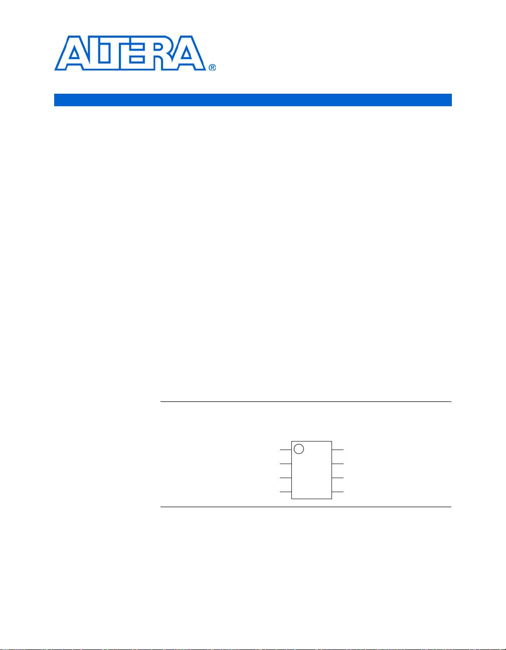
Figure 1 shows the Altera serial configuration device 8-pin SOIC package
and its pin-out diagram.
Figure 1. Altera Serial Configuration Device Package Pin-Out Diagram
1 Whenever the term “serial configuration device(s)” is used in
this document, it refers to Altera EPCS1 and EPCS4 devices.
V
CC
V
CC
DCLK
ASDI
V
CC
GND
nCS
DATA
EPCS1 or
EPCS4 Device
1
2
3
4
8
7
6
5
Serial Configuration
Devices
(EPCS1 & EPCS4)
2 Altera Corporation
Serial Configuration Devices (EPCS1 & EPCS4) Data Sheet
Functional
Description
With SRAM-based devices such as Cyclone FPGAs, configuration data
must be reloaded each time the system initializes, or when a new
configuration is needed. Serial configuration devices are flash memory
devices with a serial interface that can store configuration data for a
Cyclone device and reload the data to the device upon power-up or
reconfiguration. Table 1 lists the serial configuration devices.
Table 2 lists the serial configuration device used with each Cyclone FPGA
and the configuration file size.
Note to Table 2:
(1) These are preliminary, uncompressed file sizes.
With the new data-decompression feature in the Cyclone FPGA family,
designers can use smaller serial configuration devices to configure larger
Cyclone FPGAs. Serial configuration devices cannot be cascaded.
f
See AN 250: Configuring Cyclone FPGAs for more information regarding
the Cyclone FPGA decompression feature in AS mode.
The serial configuration devices are designed to configure Cyclone FPGAs
and cannot configure other existing device families. Figure 2 shows the
serial configuration device block diagram.
Table 1. Serial Configuration Devices (3.3-V Operation)
Device Memory Size (Bits)
EPCS1 1,048,576
EPCS4 4,194,304
Table 2. Serial Configuration Device for Cyclone Devices
Cyclone Device Configuration
File Size
(Mbits) (1)
Serial Configuration Device
EPCS1 EPCS4
EP1C3 0.628 vv
EP1C4 0.925 vv
EP1C6 1.167 vv
EP1C12 2.324 v
EP1C20 3.559 v
Altera Corporation 3
Serial Configuration Devices (EPCS1 & EPCS4) Data Sheet
Figure 2. Serial Configuration Device Block Diagram
Accessing
Memory in
Serial
Configuration
Devices
A designer can access the unused memory locations of the serial
configuration device through the Nios processor and SOPC Builder to
store/retrieve data or configuration files. SOPC Builder is an Altera tool
for creating bus-based (especially microprocessor-based) systems in
Altera devices. SOPC Builder assembles library components like
processors and memories into custom microprocessor systems.
SOPC Builder includes an interface core specifically for the serial
configuration device. Using this core, a designer can create a system with
a Nios embedded processor that allows software access to any memory
location within the serial configuration device.
f
For more information on accessing memory within the serial
configuration device, contact Altera Applications.
Control
Logic
I/O Shift
Register
Memory
Array
Status RegisterAddress Counter
Decode Logic
Data Buffer
nCS
DCLK
DATA
ASDI
Serial Configuration Device
4 Altera Corporation
Serial Configuration Devices (EPCS1 & EPCS4) Data Sheet
Pin Description
As shown in Figure 1, the serial configuration device is an 8-pin device.
The control pins on the serial configuration device are: serial data output
(DATA), active serial data input (ASDI), serial clock (DCLK), and chip select
(nCS). Table 3 shows the serial configuration device’s pin descriptions.
Programming
& Configuration
File Support
The Quartus II design software provides programming support for serial
configuration devices. After selecting the serial configuration device, the
Quartus II software automatically generates the Programmer Object File
(.pof) to program the device. The software allows users to select the
appropriate serial configuration device density that most efficiently stores
the configuration data for a selected Cyclone FPGA.
Serial configuration devices are programmed using the APU with the
appropriate programming adapter (PLMSEPC-8) via the Quartus II
software or the ByteBlaster II download cable via the Quartus II software.
In addition, many third-party programmers, such as BP Microsystems
and System General, offer programming hardware that supports serial
configuration devices.
Table 3. Serial Configuration Device Pin Description
Pin Name Pin Number Pin Type Description
DATA 2 Output DATA output signal transfers the data serially out of the serial
configuration device into the Cyclone FPGA during
read/configuration operation. During a read/configuration operation,
the serial configuration device is enabled by pulling nCS low. The
DATA signal transitions on the falling edge of DCLK.
ASDI 5 Input Active serial data input signal is used to transfer data serially into the
serial configuration device. It receives the data that should be
programmed into the serial configuration device. Values register on
the rising edge of DCLK.
nCS 1 Input Active low chip select input signal toggles at the beginning and end
of a valid instruction. When this signal is high, the device is
deselected and the DATA signal is tri-stated. When the signal is low,
it enables the device and puts the device in an active mode. After
power up, the serial configuration device requires a falling edge on
the nCS signal before beginning any operation.
DCLK 6 Input DCLK is provided by the Cyclone FPGA. This signal provides the
timing of the serial interface. The data presented at ASDI are latched
in to the serial configuration device, at the rising edge of DCLK. Data
on the DATA pin changes after the falling edge of DCLK and is latched
into the Cyclone FPGA on the rising edge.
VCC 3, 7, 8 Power Power pins connect to 3.3 V.
GND 4 Ground Ground pin.
剩余15页未读,继续阅读
资源评论
hui02_06
- 粉丝: 0
- 资源: 8
上传资源 快速赚钱
- 我的内容管理 展开
- 我的资源 快来上传第一个资源
- 我的收益 登录查看自己的收益
- 我的积分 登录查看自己的积分
- 我的C币 登录后查看C币余额
- 我的收藏
- 我的下载
- 下载帮助
最新资源
- note test a bc d e f g h
- MERGE.csv.zip
- 15白落梅:你是锦瑟我为流年:三毛的万水千山-3491776.mobi
- 微信小程序源码 实现 城市切换 demo 根据城市首字母排序城市 选择城市
- 12因为懂得 所以慈悲-张爱玲的倾城往事 (白落梅经典散文系列)-3321089.mobi
- 基于 C# 实现的串口温度监控软件
- 基于STM32F103RBT6单片机+SIM868自动收货机主控板硬件(原理图+PCB)工程文件.zip
- 微信小程序源码 车源宝 二手车交易平台 源码下载
- 专注于在线教育领域,打造更好的网课系统,网校系统,知识付费系统
- ADM487EARZ-REEL7 产品规格书pdf
资源上传下载、课程学习等过程中有任何疑问或建议,欢迎提出宝贵意见哦~我们会及时处理!
点击此处反馈
安全验证
文档复制为VIP权益,开通VIP直接复制
信息提交成功