SCT2430STER 产品规格书pdf
6 浏览量
2024-03-20
13:57:31
上传
评论
收藏 1.1MB PDF 举报

SCT2430
Rev.1.3
For more information www.silicontent.com © 2017 Silicon Content Technology Co., Ltd. All Rights Reserved 1
Product Folder Links: SCT2430
SILICON CONTENT
TECHNOLOGY
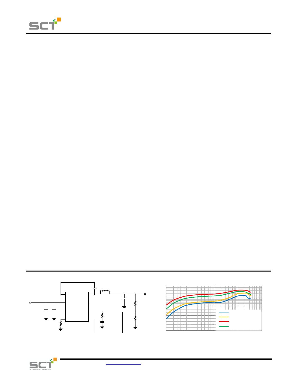
40
50
60
70
80
90
100
1 10 100 1000 10000
Efficiency(%)
Output Current(mA)
VIN=24V,VOUT=3.3V
VIN=24V,VOUT=5V
VIN=12V,VOUT=5V
VIN=12V,VOUT=3.3V
3.8V-40V Vin, 3.5A, High Efficiency Synchronous Step-down DCDC
Converter with Programmable Frequency
FEATURES
• Wide Input Range: 3.8V-40V
• Up to 3.5A Continuous Output Current
• 0.8V ±1% Feedback Reference Voltage
• Integrated 80mΩ High-Side and 50mΩ Low-Side
Power MOSFETs
• Pulse Skipping Mode (PSM) with 25uA Quiescent
Current in Sleep Mode
• 100ns Minimum On-time
• 2ms Internal Soft-start Time
• Adjustable Frequency 100KHz to 2.2MHz
• External Clock Synchronization
• Frequency Spread Spectrum (FSS) Modulation for
EMI Reduction
• Precision Enable Threshold for Programmable
Input Voltage Under-voltage Lock Out Protection
(UVLO) Threshold and Hysteresis
• Low Dropout Mode Operation
• Derivable Inverting Voltage Regulator
• Over-voltage and Over-Temperature Protection
• Available in an ESOP-8 Package
APPLICATIONS
• Battery Pack Powered System - Cordless Power
Tools, Cordless Home Appliance, Drone, Aero
Modeling, GPS Tracker etc.
• Cigarette Lighter Adapters, Chargers
• LCD Display
• USB Type-C Power Delivery, USB Charging
• Industrial and Medical Distributed Power Supplies
• Optical Communication and Networking System
• Automotive System
DESCRIPTION
The SCT2430 is 3.5A synchronous buck converters
with wide input voltage, ranging from 3.8V to 40V,
which integrates an 80mΩ high-side MOSFET and a
50mΩ low-side MOSFET. The SCT2430, adopting the
peak current mode control, supports the Pulse Skipping
Modulation (PSM) with typical 25uA low quiescent
current which assists the converter on achieving high
efficiency at light load or standby condition.
The SCT2430 features programmable switching
frequency from 100 kHz to 2.2MHz with an external
resistor, which provides the flexibility to optimize either
efficiency or external component size. The converter
supports external clock synchronization with a
frequency band from 100kHz to 2.2MHz. The SCT2430
allows power conversion from high input voltage to low
output voltage with a minimum 100ns on-time of high-
side MOSFET.
The SCT2430 is an Electromagnetic Interference (EMI)
friendly buck converter with implementing optimized
design for EMI reduction. The SCT2430 features
Frequency Spread Spectrum FSS with ±6% jittering
span of the switching frequency and modulation rate
1/512 of switching frequency to reduce the conducted
EMI.
The SCT2430 offers cycle-by-cycle current limit and
hiccup over current protection, thermal shutdown
protection, output over-voltage protection and input
voltage under-voltage protection. The device is
available in an 8-pin thermally enhanced SOP-8
package.
TYPICAL APPLICATION
BOOT
VIN
EN
RT/CLK
SW
GND
COMP
FB
SCT2430
V
IN
L1
C1 C2
R4
C5
R3
C4
R1
R2
C3
V
OUT

剩余22页未读,继续阅读
资源评论


