没有合适的资源?快使用搜索试试~ 我知道了~
GC0329 datasheet
5星 · 超过95%的资源 需积分: 48 142 下载量 66 浏览量
2012-02-13
18:02:02
上传
评论 1
收藏 1.94MB PDF 举报
温馨提示
试读
37页
GC0329是国内最大的cmos图像传感器厂商格科微电子最新推出的一款VGA sensor
资源推荐
资源详情
资源评论
1/9″VGA CMOS Image Sensor
GC0329
DataSheet
V1.0
2011-09-01
GalaxyCore Inc.
GC0329 CMOS Image Sensor
GC0329 DataSheet 2 / 37
Content
1.1 General Description .................................................................. 3
1.2 Features .................................................................................. 3
1.3 Application ............................................................................... 4
1.4 Technical Specifications ............................................................ 4
1.5 Block Diagram .......................................................................... 5
1.6 Pixel Array ............................................................................... 6
3.1 Protocol ................................................................................... 7
3.2 Serial Bus Timing ...................................................................... 8
7.1 GC0329 CSP package Top view (unit:um) ................................ 35
7.2 CSP ball description ................................................................ 35
7.3 GC0329 chip pin description .................................................... 35
7.4 CSP package mechanical drawing (unit:um) ............................. 37
1. Sensor Overview ...................................................... 3
2. Color Filter Spectral Characteristics ......................... 7
3. Two-wire Serial Bus Communication ....................... 7
4. Application ............................................................... 9
4.1 Timing ......................................................................... 9
5. DC Parameters ....................................................... 11
6. Register List ........................................................... 11
7. Pin Description ....................................................... 35
GC0329 CMOS Image Sensor
GC0329 DataSheet 3 / 37
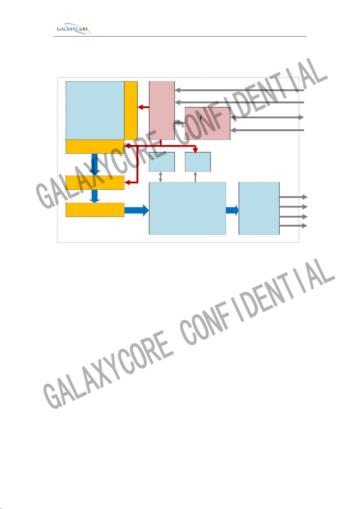
1. Sensor Overview
1.1 General Description
The GC0329 features 640V x 480H resolution with 1/9-inch optical format, and
4-transistor pixel structure for high image quality and low noise variations. It
delivers superior image quality by powerful on-chip design of a 10-bit ADC, and
embedded image signal processor.
The full scale integration of high-performance and low-power functions makes
the GC0329 best fit the design, reduce implementation process, and extend the
battery life of cell phones, PDAs, and a wide variety of mobile applications.
The on-chip ISP provides a very smooth AE (Auto Exposure) and accurate
AWB(Auto White Balance) control. It provides various data formats, such as
Bayer RGB, RGB565,YCbCr 4:2:2. It has a commonly used two-wire serial
interface for host to control the operation of the whole sensor.
1.2 Features
Standard optical format of 1/9 inch
Various output formats: YCbCr4:2:2, RGB565, Raw Bayer
Support adjusting Voltage of IO
Windowing support
Horizontal /Vertical mirror
Image processing module
Package: CSP
GC0329 CMOS Image Sensor
GC0329 DataSheet 4 / 37
1.3 Application
Cellular Phone Cameras
Notebook and desktop PC cameras
PDAs
Toys
Digital still cameras and camcorders
Video telephony and conferencing equipments
Security systems
Industrial and environmental systems
1.4 Technical Specifications
Parameter
Typical value
Optical Format
1/9 inch
Pixel Size
2.5um x 2.5um
Active pixel array
648 x 488
ADC resolution
10 bit ADC
Max Frame rate
30fps@24Mhz,VGA
Power Supply
AVDD28: 2.7 ~ 3.0V
IOVDD: 1.7 ~ 3.0V
Power Consumption
70mW @ 30fps VGA,
10μA @ standby
SNR
40dB
Dark Current
15mV/s at 60℃
Sensitivity
1.0V/(Lux·sec)
Operating temperature:
-20~70℃
Stable Image temperature
0~50℃
Optimal lens chief ray angle(CRA)
27º(linear)
Package type
CSP
GC0329 CMOS Image Sensor
GC0329 DataSheet 5 / 37
Image Signal Processing
- Interpolation
- Denoise
- Gamma
- Edge enhance
Output
Mode &
Sync
Control
Pixel Array
648H x 488V
(640H x 480V)
Row Decoder
Column CDS
Analog Processing
10bit ADC
Timing
Control
Configuration
Registers
AWB
AEC
HSYNC
VSYNC
PCLK
YUV/RGB data
RESET
SCL
MCLK
SDA
1.5 Block Diagram
GC0329 has an active image array of 648x488 pixels. The active pixels are read
out progressively through column/row driver circuits. In order to reduce fixed
pattern noise, CDS circuits are adopted. The analog signal is transferred to
digital signal by 10 bit A/D converter. The digital signals are processed in the
ISP Block, including Bayer interpolation, denoise, color correction, gamma
correction, data format conversion and so on. Users can easily control these
functions via two-wire serial interface bus.
剩余36页未读,继续阅读
hellolinran
- 粉丝: 0
- 资源: 1
上传资源 快速赚钱
- 我的内容管理 展开
- 我的资源 快来上传第一个资源
- 我的收益 登录查看自己的收益
- 我的积分 登录查看自己的积分
- 我的C币 登录后查看C币余额
- 我的收藏
- 我的下载
- 下载帮助
安全验证
文档复制为VIP权益,开通VIP直接复制
信息提交成功
- 1
- 2
- 3
- 4
- 5
前往页