没有合适的资源?快使用搜索试试~ 我知道了~
PMIC DS941 DS947 DS948
需积分: 0 3 下载量 154 浏览量
2023-03-01
08:40:41
上传
评论
收藏 9.93MB PDF 举报
温馨提示
试读
465页
最近要用的资料,上传好找
资源推荐
资源详情
资源评论
PF7100
7-channel power management integrated circuit for high
performance applications
Rev. 4 — 9 March 2021 Product data sheet
1 Overview
The PF7100 is a power management integrated circuit (PMIC) designed for high
performance i.MX 8 processors. It features five high efficiency buck converters and two
linear regulators for powering the processor, memory, and miscellaneous peripherals.
Built-in one-time programmable memory stores key startup configurations, drastically
reducing external components typically used to set output voltage and sequence of
external regulators. Regulator parameters are adjustable through high-speed I
2
C after
startup offering flexibility for different system states.
2 Features
• Five high efficiency buck converters
• Two linear regulators with load switch options
• Watchdog timer/monitor
• Monitoring circuit to fit ASIL B safety level
• One-time programmable device configuration
• 3.4 MHz I
2
C communication interface
• 48-pin 7×7 mm QFN package
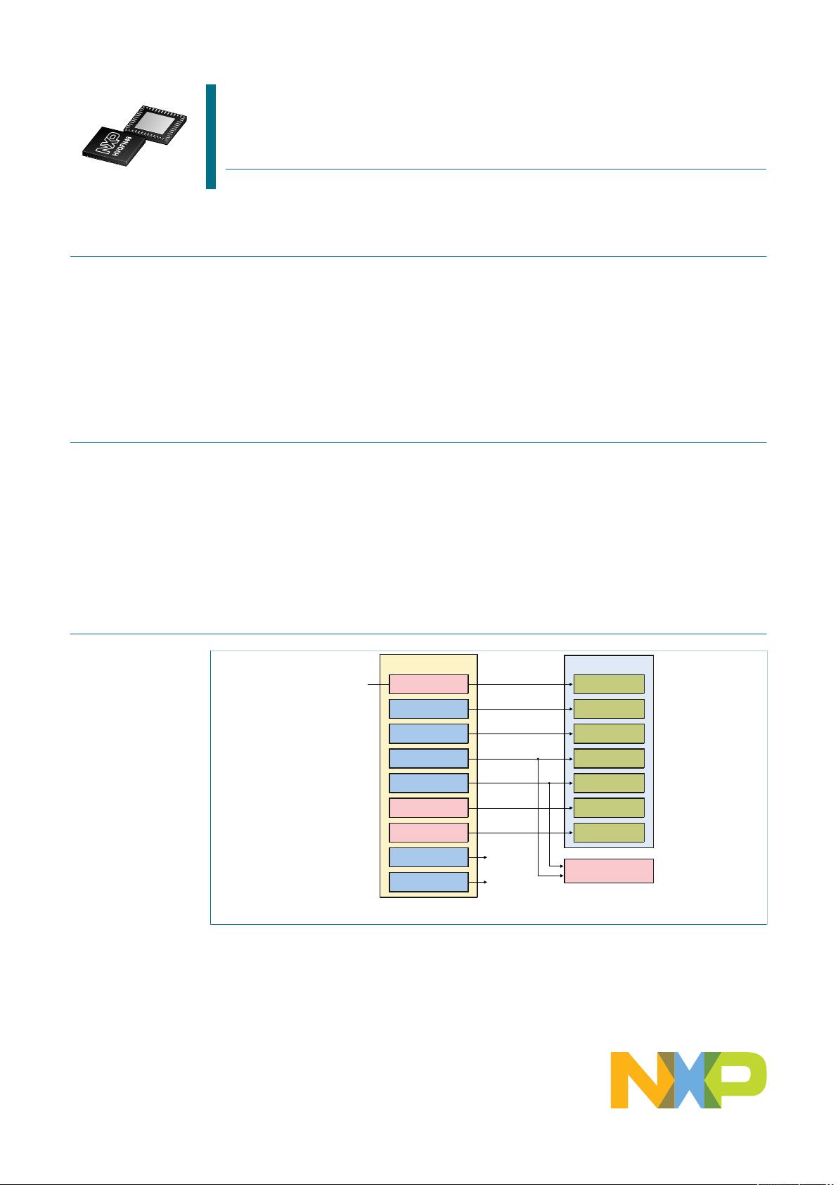
3 Simplified application diagram
aaa- 034294
VIN:
2.7 V to 5.5 V
PF7100 i.MX8xXL
VSNVS1
(3.0 V @ 10 mA)
VDD_SNVS_3P0
VDD_MAIN
BUCK1
(1.0 V @ 2.5 A)
BUCK2
(1.0 V/1.1 V @ 2.5 A)
VDD_DDR_VDDQ
BUCK4
(1.1 V/1.35 V @ 2.5 A)
VDD_1P8
BUCK5
(1.8 V @ 2.5 A)
VDD_ANA_1P8
LDO1
(
1.8 V @ 0.4 A)
VDD_SD
DDR memory
to peripherals
LDO2
(3.3 V @ 0.4 A)
BUCK3 (VTT)
(0.4 V - 1.8 V @ 2.5 A)
to peripherals
VSNVS2
(1.8 V @ 10 mA)
VDD_MEMC
Figure 1. Simplified application diagram
NXP Semiconductors
PF7100
7-channel power management integrated circuit for high performance applications
PF7100 All information provided in this document is subject to legal disclaimers. © NXP B.V. 2021. All rights reserved.
Product data sheet Rev. 4 — 9 March 2021
2 / 125
aaa- 034369
VIN:
2.7 V to 5.5 V
PF7100 i.MX8xXL
VSNVS1
(3.0 V @ 10 mA)
VDD_SNVS_3P0
VDD_MAIN
BUCK1
(1.0 V @ 2.5 A)
BUCK2
(1.0 V/1.1 V @ 2.5 A)
VDD_DDR_VDDQ
BUCK4
(1.1 V/1.35 V @ 2.5 A)
VDD_1P8
BUCK5
(1.8 V @ 2.5 A)
VDD_ANA_1P8
LDO1
(1.6 V/1.8 V @ 0.4 A)
VDD_SD
DDR memory
LDO2
(3.3 V @ 0.4 A)
BUCK3 (VTT)
(1.2 V @ 2.5 A)
VSNVS2
(1.8 V @ 10 mA)
VDD_MEMC
SAF5400
GPIO_VDD_1V8
VDDA_1V6
VDDC_1V2
Figure 2. Simplified application diagram with SAF5400 DSRC (V2X) modem
4 Ordering information
Table 1. Device information
Type Package
Name Description Version
PF7100
(automotive and industrial)
HVQFN48
HVQFN48, plastic, thermally enhanced very thin quad; flat non-leaded
package, dimple wettable flanks; 48 pins; 0.5 mm pitch; 7 mm x 7 mm
x 0.85 mm body
SOT619-27(D)
Table 2. Ordering information
Part number
[1]
Target
market
Process
or
System comments AEC-Q100
grade
[2]
Safety grade OTP ID
MPF7100BMBA0ES Automotive — OTP not programmed 1 ASIL B A0
MPF7100BVBA0ES Automotive — OTP not programmed 2 ASIL B A0
MPF7100BMMA0ES Automotive — OTP not programmed 1 QM A0
MPF7100BVMA0ES Automotive
Industrial
— OTP not programmed 2 QM A0
MPF7100BVBA1ES Automotive I.MX8XL LPDDR4 memory 2 ASIL B http://www.nxp.com/MPF7100BVBA1ES-OTP-Report
MPF7100BVMA1ES Automotive
Industrial
I.MX8XL LPDDR4 memory 2 QM http://www.nxp.com/MPF7100BVMA1ES-OTP-Report
MPF7100BVBA2ES Automotive I.MX8XL DDR3L memory 2 ASIL B http://www.nxp.com/MPF7100BVBA2ES-OTP-Report
MPF7100BVMA2ES Automotive
Industrial
I.MX8XL DDR3L memory 2 QM http://www.nxp.com/MPF7100BVMA2ES-OTP-Report
MPF7100BVBA3ES Automotive i.MX8DXP
i.MX8DX
LPDDR4 memory 2 ASIL B http://www.nxp.com/MPF7100BVBA3ES-OTP-Report
MPF7100BVMA3ES Automotive
Industrial
i.MX8DXP
i.MX8DX
LPDDR4 memory 2 QM http://www.nxp.com/MPF7100BVMA3ES-OTP-Report
MPF7100BVBA4ES Automotive i.MX8DXP
i.MX8DX
DDR3L memory 2 ASIL B http://www.nxp.com/MPF7100BVBA4ES-OTP-Report
MPF7100BVMA4ES Automotive
Industrial
i.MX8DXP
i.MX8DX
DDR3L memory 2 QM http://www.nxp.com/MPF7100BVMA4ES-OTP-Report
NXP Semiconductors
PF7100
7-channel power management integrated circuit for high performance applications
PF7100 All information provided in this document is subject to legal disclaimers. © NXP B.V. 2021. All rights reserved.
Product data sheet Rev. 4 — 9 March 2021
3 / 125
[1] To order parts in tape and reel, add the R2 suffix to the part number.
[2] For the device ambient operating temperature range, see Table 6.
5 Applications
• Automotive Infotainment
• Telematics
• High-end consumer and industrial
NXP Semiconductors
PF7100
7-channel power management integrated circuit for high performance applications
PF7100 All information provided in this document is subject to legal disclaimers. © NXP B.V. 2021. All rights reserved.
Product data sheet Rev. 4 — 9 March 2021
4 / 125
6 Internal block diagram
aaa-034296
EPAD
LDO2EN
VSELECT
SW5FB SW5IN SW5LX
Digital Signal(s)
Analog Reference(s)
20 MHz Clock/Derivative
100 kHz Clock/Derivative
LDO2
LDO1IN
LDO2OUT
LDO2 VMON
EA
AND
DRIVER
SW5 MISC
REFERENCE
SW5
VMON
LDO1
LDO1OUT
LDO2IN
SYNCIN
SYNCOUT
AMUX
AGND
DGND
VIN
VSNVS1
V1P5D
VSNVS1
VIN
OVLO
LDO1 VMON
CLOCK MANAGEMENT
(100 kHz / 20 MHz / PLL /
DIGITAL MODULE)
17 CHANNEL
ANALOG MUX
PMIC
INTERNAL
MONITORS
PGOOD
MONITORS
SW1VMON
SW2VMON
SW3VMON
SW4VMON
SW5VMON
LDO1VMON
LDO2VMON
EXTERNAL
CHANNEL
INPUT
DIE
TEMPERATURE
MONITORS
MANUAL TUNING
SPREAD SPECTRUM
EXTERNAL CLOCK
SYNC
V1P5A
FSOBPGOOD
V
BG2
V
BG1
XFAILB
V1P5D
LDO
V1P5A
LDO
REGULATION
BANDGAP
BANDGAP
COMPARATOR
MONITORING
BANDGAP
FAIL SAFE
CONTROL
VSNVS2
VSNVS2
EWARNBINTBRESETBMCU
WATCHDOG
TIMER
DIGITAL CORE
AND
STATE MACHINE
THERMAL MONITORING
/ SHUTDOWN
OTP MEMORY
WD monitoring
XINTTBBENSTANDBYPWRONWDISCLVDDIO VDDOTPSDA
V
BG2
V
BG2
V
BG2
EPAD
SW4FB
SW4IN
SW4LX
EA
AND
DRIVER
REF
SELEC.
V
BG2
SW4
VMON
EPAD
SW3FB SW3IN SW3LX
EA
AND
DRIVER
VTT
REFERENCE
SELECTOR
SW3
VMON
REF
SELEC.
SW3 DVS
AND MISC
REFERENCE
SW4 DVS
AND MISC
REFERENCE
÷ 2
V
BG2
EPAD
SW2FB
SW2IN
SW2LX
EA
AND
DRIVER
REF
SELEC.
V
BG2
SW2
VMON
SW2 DVS
AND MISC
REFERENCE
EPAD
SW1FB
SW1IN
SW1LX
EA
AND
DRIVER
REF
SELEC.
V
BG2
SW1
VMON
SW1 DVS
AND MISC
REFERENCE
Figure 3. Internal block diagram
NXP Semiconductors
PF7100
7-channel power management integrated circuit for high performance applications
PF7100 All information provided in this document is subject to legal disclaimers. © NXP B.V. 2021. All rights reserved.
Product data sheet Rev. 4 — 9 March 2021
5 / 125
7 Pinning information
7.1 Pinning
aaa-034297
V
S
E
L
EC
T
4
8
N
C
4
7
S
W
4
I
N
4
6
S
W
4
L
X
4
5
S
W
3
L
X
4
4
S
W
3
I
N
4
3
S
W
2
I
N
4
2
S
W
2
L
X
4
1
S
W
1
L
X
4
0
S
W
1
I
N
3
9
P
G
O
O
D
3
8
I
N
T
B
3
7
FSOB
36
RESETBMCU
35
PWRON
34
STANDBY
33
TBBEN
32
SW1FB
31
SW2FB
30
DGND
29
V1P5D
28
VIN
27
AGND
26
AMUX
25
XINTB
13
NC1
14
SW5IN
15
SW5LX
16
XFAILB
17
LDO2OUT
18
LDO2IN
19
LDO1IN
20
LDO1OUT
21
VSNVS2
22
VSNVS1
23
V1P5A
24
WDI
1
SYNCOUT
2
EWARN
3
LDO2EN
4
SYNCIN
5
SW4FB
6
SW3FB
EPAD
7
VDDOTP
8
VDDIO
9
SDA
10
SCL
11
SW5FB
12
Figure 4. Pin configuration for HVQFN48
7.2 Pin definitions
Table 3. Pin definitions
Pin number Symbol Application description Pin type Min Max Units
1 WDI Watchdog Input from MCU I −0.3 6.0 V
2 SYNCOUT Clock out pin for external part synchronization O −0.3 6.0 V
3 EWARN Early warning to MCU O −0.3 6.0 V
4 LDO2EN LDO2 enable pin I −0.3 6.0 V
5 SYNCIN External clock input pin for synchronization I −0.3 6.0 V
6 SW4FB Buck 4 output voltage feedback I −0.3 6.0 V
7 SW3FB Buck 3 output voltage feedback I −0.3 6.0 V
8 VDDOTP OTP selection input I −0.3 10 V
9 VDDIO I/O supply voltage. Connect to voltage rail between 1.6 V and 3.3 V. I −0.3 6.0 V
10 SDA I
2
C data signal I/O −0.3 6.0 V
11 SCL I
2
C clock signal I −0.3 6.0 V
12 SW5FB Buck 5 output voltage feedback I −0.3 6.0 V
13 XINTB External interrupt input I −0.3 6.0 V
14 NC1 Reserved — — — —
15 SW5IN Buck 5 input supply I −0.3 6.0 V
剩余464页未读,继续阅读
资源评论
gxl
- 粉丝: 11
- 资源: 22
上传资源 快速赚钱
- 我的内容管理 展开
- 我的资源 快来上传第一个资源
- 我的收益 登录查看自己的收益
- 我的积分 登录查看自己的积分
- 我的C币 登录后查看C币余额
- 我的收藏
- 我的下载
- 下载帮助
安全验证
文档复制为VIP权益,开通VIP直接复制
信息提交成功