


MPC5748G Reference Manual
Supports MPC5747C, MPC5748C, MPC5746G, MPC5747G, and
MPC5748G
Document Number: MPC5748GRM
Rev. 7.1, 01/2019

MPC5748G Reference Manual, Rev. 7.1, 01/2019
2 NXP Semiconductors

Contents
Section number Title Page
Chapter 1
About This Manual
1.1 Audience....................................................................................................................................................................... 103
1.2 Organization..................................................................................................................................................................103
1.2.1 Attachments................................................................................................................................................. 103
1.3 Module descriptions......................................................................................................................................................103
1.3.1 Example: chip-specific information that clarifies content in the same chapter........................................... 104
1.3.2 Example: chip-specific information that refers to a different chapter......................................................... 105
1.4 Register descriptions.....................................................................................................................................................106
1.5 Conventions.................................................................................................................................................................. 107
1.5.1 Notes, Cautions, and Warnings....................................................................................................................107
1.5.2 Numbering systems......................................................................................................................................107
1.5.3 Typographic notation................................................................................................................................... 108
1.5.4 Special terms................................................................................................................................................108
Chapter 2
Introduction
2.1 Introduction...................................................................................................................................................................111
2.1.1 Target Applications......................................................................................................................................111
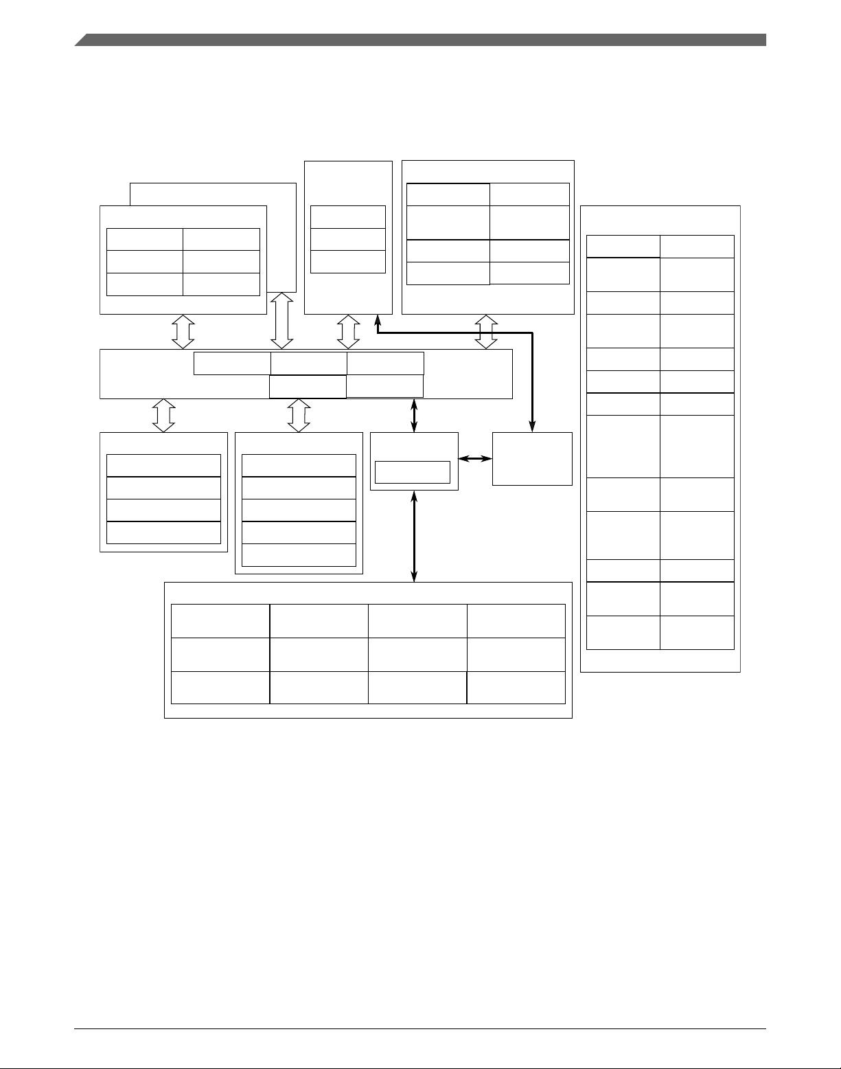
2.2 Block diagram...............................................................................................................................................................111
2.3 Family comparison........................................................................................................................................................112
2.4 Feature list.....................................................................................................................................................................117
2.5 Package Options............................................................................................................................................................119
2.6 Modes of Operation...................................................................................................................................................... 119
Chapter 3
Memory Map
3.1 Introduction...................................................................................................................................................................125
3.2 System memory map.....................................................................................................................................................125
3.3 NVM memory map.......................................................................................................................................................126
MPC5748G Reference Manual, Rev. 7.1, 01/2019
NXP Semiconductors 3
Section number Title Page
3.4 UTEST Memory Map...................................................................................................................................................128
3.5 RAM memory map....................................................................................................................................................... 129
3.6 Peripheral Bridges A and B memory maps...................................................................................................................130
3.6.1 Peripheral Bridge A memory map............................................................................................................... 130
3.6.2 Peripheral Bridge B memory map............................................................................................................... 133
3.7 MC_CGM mapped peripherals memory map...............................................................................................................134
3.8 PCU mapped peripherals memory map........................................................................................................................ 135
3.9 DMAMUX mapped peripherals memory map............................................................................................................. 135
Chapter 4
Signal Description
4.1 Generic pins/balls..........................................................................................................................................................137
4.1.1 MSCR assignments......................................................................................................................................137
4.2 PAD keeping feature in LPU/STANDBY mode.......................................................................................................... 138
Chapter 5
Security Overview
5.1 Introduction...................................................................................................................................................................143
5.2 Basic security................................................................................................................................................................143
5.3 Advanced security.........................................................................................................................................................143
5.4 Detailed security information....................................................................................................................................... 144
Chapter 6
Platform Overview
6.1 Introduction...................................................................................................................................................................145
6.2 Performance Enhancement........................................................................................................................................... 146
6.3 User/Privilege Access................................................................................................................................................... 147
6.4 Endianess control..........................................................................................................................................................148
Chapter 7
Power Management Overview
7.1 Introduction...................................................................................................................................................................151
7.1.1 Features........................................................................................................................................................ 152
7.2 Power domains..............................................................................................................................................................153
MPC5748G Reference Manual, Rev. 7.1, 01/2019
4 NXP Semiconductors
Section number Title Page
7.2.1 Power Domain0 (PD0).................................................................................................................................154
7.2.2 Power Domain1 (PD1).................................................................................................................................154
7.2.3 Power Domain2 (PD2).................................................................................................................................154
7.2.4 Flash HV power domain.............................................................................................................................. 155
7.2.5 SRAM domains............................................................................................................................................155
7.2.6 SRAM Configuration...................................................................................................................................155
7.3 User operating modes, power domains, and clock gating............................................................................................ 156
7.4 Voltage regulators.........................................................................................................................................................158
7.4.1 FPREG voltage regulator.............................................................................................................................158
7.4.2 LPREG voltage regulator.............................................................................................................................160
7.4.3 ULPREG voltage regulator..........................................................................................................................160
7.4.4 Flash voltage regulator.................................................................................................................................161
7.4.5 Voltage monitoring...................................................................................................................................... 161
7.4.6 Applications and Low Power Modes...........................................................................................................163
7.5 External Regulation...................................................................................................................................................... 164
7.5.1 PORST in EXTERNAL REGULATION.................................................................................................... 164
7.5.2 External regulator contol..............................................................................................................................164
7.6 Accelerated Low Power Exit........................................................................................................................................ 166
Chapter 8
Low Power Subsystem (LPU)
8.1 Introduction...................................................................................................................................................................169
8.2 Block diagram...............................................................................................................................................................169
8.3 Features.........................................................................................................................................................................170
8.4 Modes of operation....................................................................................................................................................... 172
8.5 Transition to LPU mode................................................................................................................................................173
8.6 Exit from LPU Modes...................................................................................................................................................177
8.7 Clocking........................................................................................................................................................................178
8.7.1 LPU System Clock Generation....................................................................................................................178
8.7.2 FlexCAN0 Clocking.................................................................................................................................... 180
MPC5748G Reference Manual, Rev. 7.1, 01/2019
NXP Semiconductors 5


