
1. General description
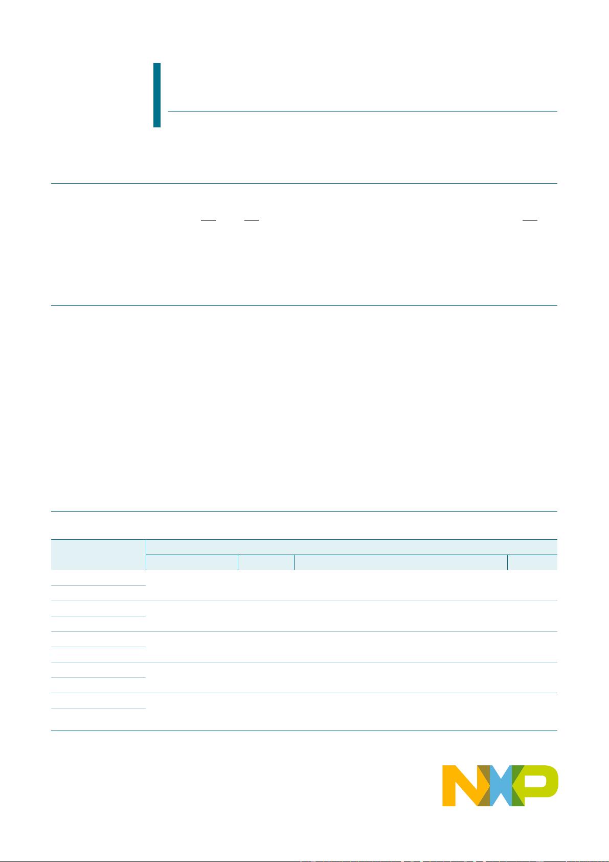
The 74HC244; 74HCT244 is an 8-bit buffer/line driver with 3-state outputs. The device
can be used as two 4-bit buffers or one 8-bit buffer. The device features two output
enables (1OE
and 2OE), each controlling four of the 3-state outputs. A HIGH on nOE
causes the outputs to assume a high-impedance OFF-state. Inputs include clamp diodes
that enable the use of current limiting resistors to interface inputs to voltages in excess of
V
CC
.
2. Features and benefits
Input levels:
For 74HC244: CMOS level
For 74HCT244: TTL level
Octal bus interface
Non-inverting 3-state outputs
Complies with JEDEC standard no. 7 A
ESD protection:
HBM JESD22-A114F exceeds 2000 V
MM JESD22-A115-A exceeds 200 V
Multiple package options
Specified from 40 Cto +85C and 40 Cto +125C
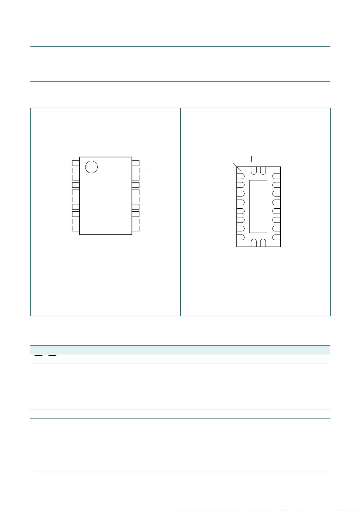
3. Ordering information
74HC244; 74HCT244
Octal buffer/line driver; 3-state
Rev. 4 — 24 September 2012 Product data sheet
Table 1. Ordering information
Type number Package
Temperature range Name Description Version
74HC244N 40 Cto+125C DIP20 plastic dual in-line package; 20 leads (300 mil) SOT146-1
74HCT244N
74HC244D 40 Cto+125C SO20 plastic small outline package; 20 leads;
body width 7.5 mm
SOT163-1
74HCT244D
74HC244DB 40 Cto+125C SSOP20 plastic shrink small outline package; 20 leads;
body width 5.3 mm
SOT339-1
74HCT244DB
74HC244PW 40 Cto+125C TSSOP20 plastic thin shrink small outline package; 20 leads;
body width 4.4 mm
SOT360-1
74HCT244PW
74HC244BQ 40 C to +125 C DHVQFN20 plastic dual-in-line compatible thermal enhanced
very thin quad flat package; no leads; 20 terminals;
body 2.5 4.5 0.85 mm
SOT764-1
74HCT244BQ
剩余17页未读,继续阅读
资源评论


ZoeyCool
- 粉丝: 3
- 资源: 23


最新资源
- java毕设项目之基于ssm框架的博客系统的开发+vue(完整前后端+说明文档+mysql+lw).zip
- java毕设项目之基于ssm框架的校园闲置物品交易平台+jsp(完整前后端+说明文档+mysql+lw).zip
- java毕设项目之基于vue.js的购物商场的设计与实现+vue(完整前后端+说明文档+mysql+lw).zip
- 生菜生长记录数据集(3K+ 记录,7特征) CSV
- java毕设项目之基于协同过滤技术的网上书城的开发与研究+jsp(完整前后端+说明文档+mysql+lw).zip
- 微信小程序商城,微信小程序demo
- java毕设项目之教务信息平台的设计与实现+jsp(完整前后端+说明文档+mysql+lw).zip
- java毕设项目之江苏融汇房地产营销策划有限公司的宣传网站+vue(完整前后端+说明文档+mysql+lw).zip
- 【计算机网络基础】章节测试1+概述.html
- 大学录取结果数据集,大学录取结果分析数据,大学录取因素分析
- java毕设项目之课程在线教学平台设计与实现+jsp(完整前后端+说明文档+mysql+lw).zip
- Android开发工程师张某某的详细个人简历
- MySQL数据库从入门到精通的学习资源汇总
- 常用成语汇编-1768常用词条收录-1.7万成语汇总
- CA51F3系列MCU参考电路,LCD,LED参考电路设计 REV 2.0
- java毕设项目之新媒体视域下的中国古诗词展演+vue(完整前后端+说明文档+mysql+lw).zip
资源上传下载、课程学习等过程中有任何疑问或建议,欢迎提出宝贵意见哦~我们会及时处理!
点击此处反馈


