没有合适的资源?快使用搜索试试~ 我知道了~
资源详情
资源评论
资源推荐
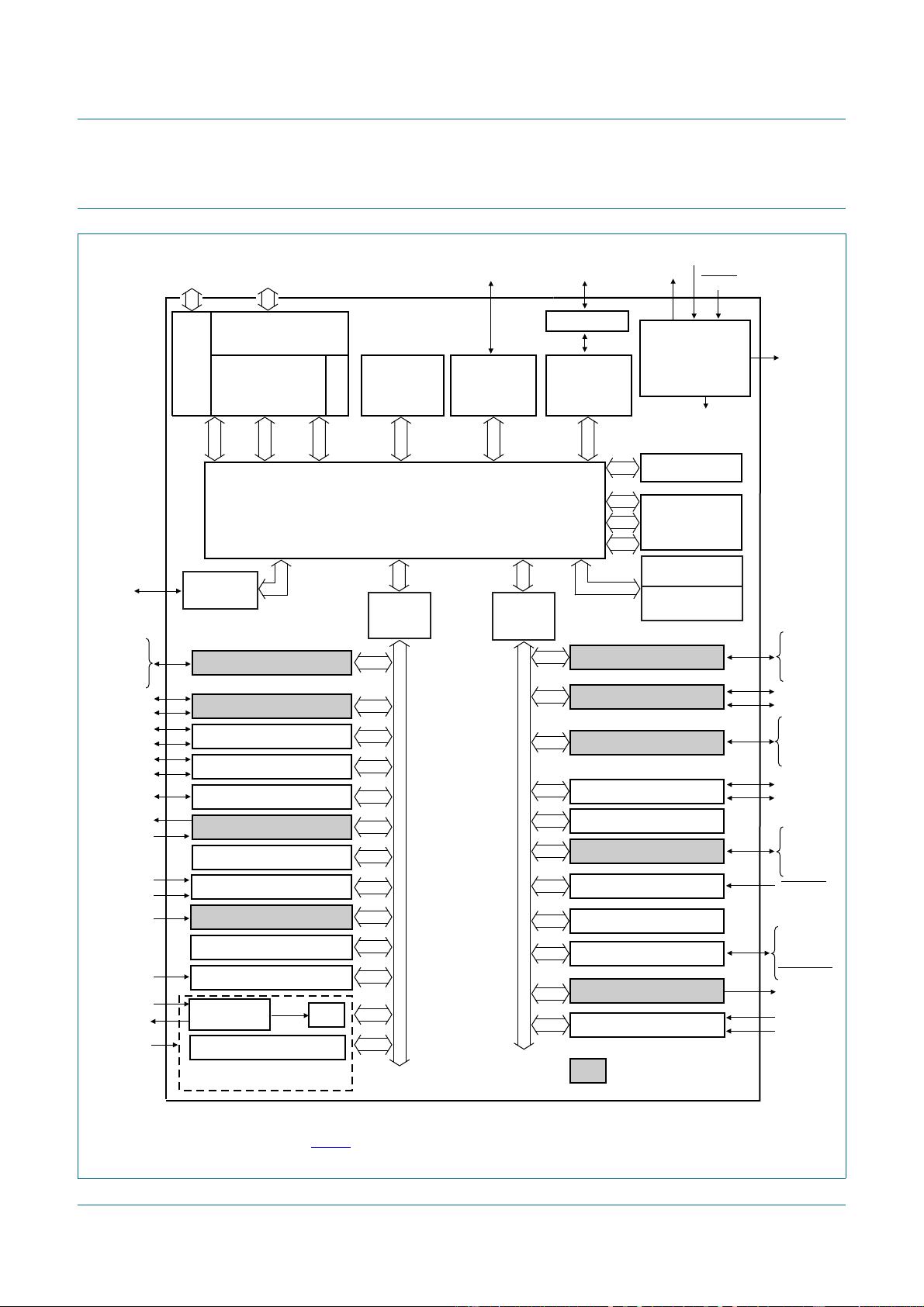
1. General description
The LPC1769/68/67/66/65/64/63 are ARM Cortex-M3 based microcontrollers for
embedded applications featuring a high level of integration and low power consumption.
The ARM Cortex-M3 is a next generation core that offers system enhancements such as
enhanced debug features and a higher level of support block integration.
The LPC1768/67/66/65/64/63 operate at CPU frequencies of up to 100 MHz. The
LPC1769 operates at CPU frequencies of up to 120 MHz. The ARM Cortex-M3 CPU
incorporates a 3-stage pipeline and uses a Harvard architecture with separate local
instruction and data buses as well as a third bus for peripherals. The ARM Cortex-M3
CPU also includes an internal prefetch unit that supports speculative branching.
The peripheral complement of the LPC1769/68/67/66/65/64/63 includes up to 512 kB of
flash memory, up to 64 kB of data memory, Ethernet MAC, USB Device/Host/OTG
interface, 8-channel general purpose DMA controller, 4 UARTs, 2 CAN channels, 2 SSP
controllers, SPI interface, 3 I
2
C-bus interfaces, 2-input plus 2-output I
2
S-bus interface,
8-channel 12-bit ADC, 10-bit DAC, motor control PWM, Quadrature Encoder interface,
four general purpose timers, 6-output general purpose PWM, ultra-low power Real-Time
Clock (RTC) with separate battery supply, and up to 70 general purpose I/O pins.
The LPC1769/68/67/66/65/64/63 are pin-compatible to the 100-pin LPC236x
ARM7-based microcontroller series.
2. Features and benefits
ARM Cortex-M3 processor, running at frequencies of up to 100 MHz
(LPC1768/67/66/65/64/63) or of up to 120 MHz (LPC1769). A Memory Protection Unit
(MPU) supporting eight regions is included.
ARM Cortex-M3 built-in Nested Vectored Interrupt Controller (NVIC).
Up to 512 kB on-chip flash programming memory. Enhanced flash memory accelerator
enables high-speed 120 MHz operation with zero wait states.
In-System Programming (ISP) and In-Application Programming (IAP) via on-chip
bootloader software.
On-chip SRAM includes:
32/16 kB of SRAM on the CPU with local code/data bus for high-performance CPU
access.
LPC1769/68/67/66/65/64/63
32-bit ARM Cortex-M3 microcontroller; up to 512 kB flash and
64 kB SRAM with Ethernet, USB 2.0 Host/Device/OTG, CAN
Rev. 9 — 10 August 2012 Product data sheet
LPC1769_68_67_66_65_64_63 All information provided in this document is subject to legal disclaimers. © NXP B.V. 2012. All rights reserved.
Product data sheet Rev. 9.0 — 10 August 2012 2 of 82
NXP Semiconductors
LPC1769/68/67/66/65/64/63
32-bit ARM Cortex-M3 microcontroller
Two/one 16 kB SRAM blocks with separate access paths for higher throughput.
These SRAM blocks may be used for Ethernet, USB, and DMA memory, as well as
for general purpose CPU instruction and data storage.
Eight channel General Purpose DMA controller (GPDMA) on the AHB multilayer
matrix that can be used with SSP, I
2
S-bus, UART, Analog-to-Digital and
Digital-to-Analog converter peripherals, timer match signals, and for
memory-to-memory transfers.
Multilayer AHB matrix interconnect provides a separate bus for each AHB master.
AHB masters include the CPU, General Purpose DMA controller, Ethernet MAC, and
the USB interface. This interconnect provides communication with no arbitration
delays.
Split APB bus allows high throughput with few stalls between the CPU and DMA.
Serial interfaces:
Ethernet MAC with RMII interface and dedicated DMA controller. (Not available on
all parts, see Table 2
.)
USB 2.0 full-speed device/Host/OTG controller with dedicated DMA controller and
on-chip PHY for device, Host, and OTG functions. (Not available on all parts, see
Table 2
.)
Four UARTs with fractional baud rate generation, internal FIFO, and DMA support.
One UART has modem control I/O and RS-485/EIA-485 support, and one UART
has IrDA support.
CAN 2.0B controller with two channels. (Not available on all parts, see Table 2
.)
SPI controller with synchronous, serial, full duplex communication and
programmable data length.
Two SSP controllers with FIFO and multi-protocol capabilities. The SSP interfaces
can be used with the GPDMA controller.
Three enhanced I
2
C bus interfaces, one with an open-drain output supporting full
I
2
C specification and Fast mode plus with data rates of 1 Mbit/s, two with standard
port pins. Enhancements include multiple address recognition and monitor mode.
I
2
S (Inter-IC Sound) interface for digital audio input or output, with fractional rate
control. The I
2
S-bus interface can be used with the GPDMA. The I
2
S-bus interface
supports 3-wire and 4-wire data transmit and receive as well as master clock
input/output. (Not available on all parts, see Table 2
.)
Other peripherals:
70 (100 pin package) General Purpose I/O (GPIO) pins with configurable
pull-up/down resistors. All GPIOs support a new, configurable open-drain operating
mode. The GPIO block is accessed through the AHB multilayer bus for fast access
and located in memory such that it supports Cortex-M3 bit banding and use by the
General Purpose DMA Controller.
12-bit Analog-to-Digital Converter (ADC) with input multiplexing among eight pins,
conversion rates up to 200 kHz, and multiple result registers. The 12-bit ADC can
be used with the GPDMA controller.
10-bit Digital-to-Analog Converter (DAC) with dedicated conversion timer and DMA
support. (Not available on all parts, see Table 2
)
Four general purpose timers/counters, with a total of eight capture inputs and ten
compare outputs. Each timer block has an external count input. Specific timer
events can be selected to generate DMA requests.
One motor control PWM with support for three-phase motor control.
LPC1769_68_67_66_65_64_63 All information provided in this document is subject to legal disclaimers. © NXP B.V. 2012. All rights reserved.
Product data sheet Rev. 9.0 — 10 August 2012 3 of 82
NXP Semiconductors
LPC1769/68/67/66/65/64/63
32-bit ARM Cortex-M3 microcontroller
Quadrature encoder interface that can monitor one external quadrature encoder.
One standard PWM/timer block with external count input.
RTC with a separate power domain and dedicated RTC oscillator. The RTC block
includes 20 bytes of battery-powered backup registers.
WatchDog Timer (WDT). The WDT can be clocked from the internal RC oscillator,
the RTC oscillator, or the APB clock.
ARM Cortex-M3 system tick timer, including an external clock input option.
Repetitive interrupt timer provides programmable and repeating timed interrupts.
Each peripheral has its own clock divider for further power savings.
Standard JTAG test/debug interface for compatibility with existing tools. Serial Wire
Debug and Serial Wire Trace Port options.
Emulation trace module enables non-intrusive, high-speed real-time tracing of
instruction execution.
Integrated PMU (Power Management Unit) automatically adjusts internal regulators to
minimize power consumption during Sleep, Deep sleep, Power-down, and Deep
power-down modes.
Four reduced power modes: Sleep, Deep-sleep, Power-down, and Deep power-down.
Single 3.3 V power supply (2.4 V to 3.6 V).
Four external interrupt inputs configurable as edge/level sensitive. All pins on Port 0
and Port 2 can be used as edge sensitive interrupt sources.
Non-maskable Interrupt (NMI) input.
Clock output function that can reflect the main oscillator clock, IRC clock, RTC clock,
CPU clock, and the USB clock.
The Wake-up Interrupt Controller (WIC) allows the CPU to automatically wake up from
any priority interrupt that can occur while the clocks are stopped in deep sleep,
Power-down, and Deep power-down modes.
Processor wake-up from Power-down mode via any interrupt able to operate during
Power-down mode (includes external interrupts, RTC interrupt, USB activity, Ethernet
wake-up interrupt, CAN bus activity, Port 0/2 pin interrupt, and NMI).
Brownout detect with separate threshold for interrupt and forced reset.
Power-On Reset (POR).
Crystal oscillator with an operating range of 1 MHz to 25 MHz.
4 MHz internal RC oscillator trimmed to 1 % accuracy that can optionally be used as a
system clock.
PLL allows CPU operation up to the maximum CPU rate without the need for a
high-frequency crystal. May be run from the main oscillator, the internal RC oscillator,
or the RTC oscillator.
USB PLL for added flexibility.
Code Read Protection (CRP) with different security levels.
Unique device serial number for identification purposes.
Available as LQFP100 (14 mm 14 mm 1.4 mm) and TFBGA100
1
(9 mm 9 mm
0.7 mm) package.
1. LPC1768/65 only.
LPC1769_68_67_66_65_64_63 All information provided in this document is subject to legal disclaimers. © NXP B.V. 2012. All rights reserved.
Product data sheet Rev. 9.0 — 10 August 2012 4 of 82
NXP Semiconductors
LPC1769/68/67/66/65/64/63
32-bit ARM Cortex-M3 microcontroller
3. Applications
4. Ordering information
4.1 Ordering options
eMetering Alarm systems
Lighting White goods
Industrial networking Motor control
Table 1. Ordering information
Type number Package
Name Description Version
LPC1769FBD100 LQFP100 plastic low profile quad flat package; 100 leads; body 14 14 1.4 mm SOT407-1
LPC1768FBD100 LQFP100 plastic low profile quad flat package; 100 leads; body 14 14 1.4 mm SOT407-1
LPC1768FET100 TFBGA100 plastic thin fine-pitch ball grid array package; 100 balls; body 9 9 0.7 mm SOT926-1
LPC1767FBD100 LQFP100 plastic low profile quad flat package; 100 leads; body 14 14 1.4 mm SOT407-1
LPC1766FBD100 LQFP100 plastic low profile quad flat package; 100 leads; body 14 14 1.4 mm SOT407-1
LPC1765FBD100 LQFP100 plastic low profile quad flat package; 100 leads; body 14 14 1.4 mm SOT407-1
LPC1765FET100 TFBGA100 plastic thin fine-pitch ball grid array package; 100 balls; body 9 9 0.7 mm SOT926-1
LPC1764FBD100 LQFP100 plastic low profile quad flat package; 100 leads; body 14 14 1.4 mm SOT407-1
LPC1763FBD100 LQFP100 plastic low profile quad flat package; 100 leads; body 14 14 1.4 mm SOT407-1
Table 2. Ordering options
Type number Flash SRAM in kB Ethernet USB CAN I
2
S DAC Maximum
CPU
operating
frequency
CPU AHB
SRAM0
AHB
SRAM1
Total
LPC1769FBD100 512 kB 32 16 16 64 yes Device/Host/OTG 2 yes yes 120 MHz
LPC1768FBD100 512 kB 32 16 16 64 yes Device/Host/OTG 2 yes yes 100 MHz
LPC1768FET100 512 kB 32 16 16 64 yes Device/Host/OTG 2 yes yes 100 MHz
LPC1767FBD100 512 kB 32 16 16 64 yes no no yes yes 100 MHz
LPC1766FBD100 256 kB 32 16 16 64 yes Device/Host/OTG 2 yes yes 100 MHz
LPC1765FBD100 256 kB 32 16 16 64 no Device/Host/OTG 2 yes yes 100 MHz
LPC1765FET100 256 kB 32 16 16 64 no Device/Host/OTG 2 yes yes 100 MHz
LPC1764FBD100 128 kB 16 16 - 32 yes Device only 2 no no 100 MHz
LPC1763FBD100 256 kB 32 16 16 64 no no no yes yes 100 MHz
LPC1769_68_67_66_65_64_63 All information provided in this document is subject to legal disclaimers. © NXP B.V. 2012. All rights reserved.
Product data sheet Rev. 9.0 — 10 August 2012 5 of 82
NXP Semiconductors
LPC1769/68/67/66/65/64/63
32-bit ARM Cortex-M3 microcontroller
5. Block diagram
(1) Not available on all parts. See Tabl e 2.
Fig 1. Block diagram
SRAM 32/64 kB
ARM
CORTEX-M3
TEST/DEBUG
INTERFACE
EMULATION
TRACE MODULE
FLASH
ACCELERATOR
FLASH
512/256/128 kB
DMA
CONTROLLER
ETHERNET
CONTROLLER
WITH DMA
(1)
USB HOST/
DEVICE/OTG
CONTROLLER
WITH DMA
(1)
I-code
bus
D-code
bus
system
bus
AHB TO
APB
BRIDGE 0
HIGH-SPEED
GPIO
AHB TO
APB
BRIDGE 1
CLOCK
GENERATION,
POWER CONTROL,
SYSTEM
FUNCTIONS
XTAL1
XTAL2
RESET
clocks and
controls
JTAG
interface
debug
port
USB PHY
SSP0
UART2/3
I2S
(1)
I2C2
RI TIMER
TIMER2/3
EXTERNAL INTERRUPTS
SYSTEM CONTROL
MOTOR CONTROL PWM
QUADRATURE ENCODER
SSP1
UART0/1
CAN1/2
(1)
I2C0/1
SPI0
TIMER 0/1
WDT
PWM1
12-bit ADC
PIN CONNECT
GPIO INTERRUPT CONTROL
RTC
BACKUP REGISTERS
32 kHz
OSCILLATOR
APB slave group 1
APB slave group 0
DAC
(1)
RTC POWER DOMAIN
LPC1769/68/67/
66/65/64/63
master master master
002aad944
slaveslave slave
slave
slave
ROM
slave
MULTILAYER AHB MATRIX
P0 to
P4
SDA2
SCL2
SCK0
SSEL0
MISO0
MOSI0
SCK1
SSEL1
MISO1
MOSI1
RXD2/3
TXD2/3
PHA, PHB
INDEX
EINT[3:0]
AOUT
MCOA[2:0]
MCOB[2:0]
MCI[2:0]
MCABORT
4 × MAT2
2 × MAT3
2 × CAP2
2 × CAP3
3 × I2SRX
3 × I2STX
TX_MCLK
RX_MCLK
RTCX1
RTCX2
VBAT
PWM1[7:0]
2 × MAT0/1
2 × CAP0/1
RD1/2
TD1/2
SDA0/1
SCL0/1
AD0[7:0]
SCK/SSEL
MOSI/MISO
8 × UART1
RXD0/TXD0
P0, P2
PCAP1[1:0]
RMII pins
USB pins
CLKOUT
MPU
= connected to DMA
剩余81页未读,继续阅读
gqb666
- 粉丝: 439
- 资源: 122
上传资源 快速赚钱
- 我的内容管理 展开
- 我的资源 快来上传第一个资源
- 我的收益 登录查看自己的收益
- 我的积分 登录查看自己的积分
- 我的C币 登录后查看C币余额
- 我的收藏
- 我的下载
- 下载帮助
最新资源
- MyBatis动态SQL是一种强大的特性,它允许我们在SQL语句中根据条件动态地添加或删除某些部分,从而实现更加灵活和高效的数据
- Docker在Ubuntu16.04上安装和部署Apache Storm
- test_kong.zip
- springboot权限验证学习-下
- SeetaFace6人脸质量评估C++代码实现Demo
- OCAuxiliaryTools
- 制药公司QC顶岗实习专题报告
- Rust 全面指南:从基础到高级,一网打尽 Rust 的编程知识
资源上传下载、课程学习等过程中有任何疑问或建议,欢迎提出宝贵意见哦~我们会及时处理!
点击此处反馈
安全验证
文档复制为VIP权益,开通VIP直接复制
信息提交成功
评论0