没有合适的资源?快使用搜索试试~ 我知道了~
GATE DRIVE REQUIREMENTS OF HIGH-SIDE DEVICES A TYPICAL BLOCK DIAGRAM HOW TO SELECT THE BOOTSTRAP COMPONENTS HOW TO CALCULATE THE POWER DISSIPATION IN AN MGD HOW TO PROVIDE A CONTINUOUS GATE DRIVE HOW TO GENERATE A NEGATIVE GATE BIAS HOW TO DRIVE A BUCK CONVERTER
资源推荐
资源详情
资源评论
![pdf](https://img-home.csdnimg.cn/images/20210720083512.png)
![rar](https://img-home.csdnimg.cn/images/20210720083606.png)
![doc](https://img-home.csdnimg.cn/images/20210720083327.png)
![pdf](https://img-home.csdnimg.cn/images/20210720083512.png)
![zip](https://img-home.csdnimg.cn/images/20210720083736.png)
![pptx](https://img-home.csdnimg.cn/images/20210720083543.png)
![zip](https://img-home.csdnimg.cn/images/20210720083736.png)
![doc](https://img-home.csdnimg.cn/images/20210720083327.png)
![zip](https://img-home.csdnimg.cn/images/20210720083736.png)
![pptx](https://img-home.csdnimg.cn/images/20210720083543.png)
![pdf](https://img-home.csdnimg.cn/images/20210720083512.png)
![rar](https://img-home.csdnimg.cn/images/20210720083606.png)
![zip](https://img-home.csdnimg.cn/images/20210720083736.png)
![7z](https://img-home.csdnimg.cn/images/20210720083312.png)
![zip](https://img-home.csdnimg.cn/images/20210720083736.png)
![pdf](https://img-home.csdnimg.cn/images/20210720083512.png)
![rplib](https://img-home.csdnimg.cn/images/20210720083646.png)
![](https://csdnimg.cn/release/download_crawler_static/89128291/bg1.jpg)
A
PPLICATION
N
OTE
1. GATE DRIVE REQUIREMENTS OF HIGH-SIDE DEVICES
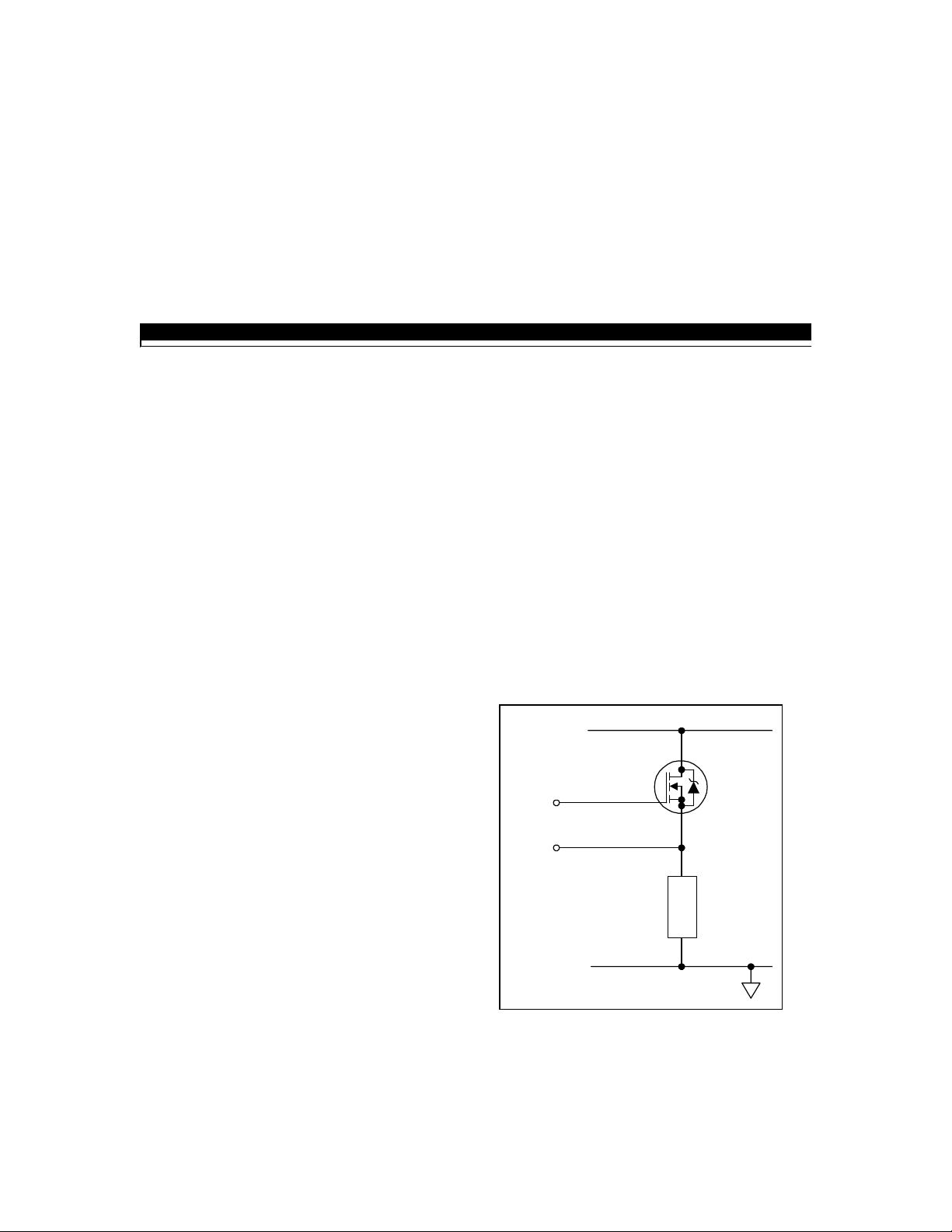
The gate drive requirements for a power MOSFET or IGBT uti-
lized as a high side switch (drain connected to the high voltage
rail, as shown in Figure 1) driven in full enhancement, i.e., lowest
voltage drop across its terminals, can be summarized as follows:
1. Gate voltage must be 10-15V higher than the
drain voltage. Being a high side switch, such
gate voltage would have to be higher than the
rail voltage, which is frequently the highest volt-
age available in the system.
2. The gate voltage must be controllable from the
logic, which is normally referenced to ground.
Thus, the control signals have to be level-shifted
to the source of the high side power device,
which, in most applications, swings between the
two rails.
3. The power absorbed by the gate drive circuitry
should not significantly affect the overall effi-
ciency.
With these constraints in mind, several techniques are presently
used to perform this function, as shown in principle in Table I.
Each basic circuit can be implemented in a wide variety of con-
figurations.
HV Floating MOS-Gate Driver ICs
(HEXFET is a trademark of International Rectifier)
How to provide a negative gate drive
Driving Buck converters
Driving Dual-Forwards and switched reluctance
motor controllers
Cycle-by-cycle current control by means of the SD
pin
Brushless and induction motor drives
Push-pull and other low-side applications
Driving a high-side P-Channel MOSFET
How to drive thyristor gates
Troubleshooting guidelines
Topics Covered:
Gate drive requirements of high side devices
Block diagram of a typical MGD
Bootstrap operation
How to select the bootstrap components
How to calculate the power dissipation in the MGD
How to deal with negative transients
Layouts and other guidelines
How to isolate the logic from the power circuit
How to boost the output current of an MGD to drive
modules
How to provide a continuous gate drive
GATE
SOURCE
V
+
HIGH VOLTAGE RAIL
Figure 1.
Power MOSFET in high side
configuration
www.irf.com 1
![](https://csdnimg.cn/release/download_crawler_static/89128291/bg2.jpg)
2
V
DD
H
IN
SD
L
IN
V
SS
R
S
R
S
V
DD
/ V
CC
LEVEL
TRANSLATOR
AND PW
DISCRIMINATOR
PULSE
GENERATOR
UV
DETECT
DELAY
V
DD
/ V
BS
LEVEL
TRANSLATOR
PULSE
DISCRIMINATOR
C
d-sub
C
b-sub
UV
DETECT
LATCH
LOGIC
Q
Q
V
B
HO
V
S
LO
2
COMM
C
BOOT
V
CC
V
R
V
DD
/ V
CC
LEVEL
TRANSLATOR
AND PW
DISCRIMINATOR
Figure 2.
Block Diagram of the IR2110
HIGH SIDE
CMOS
LD MOS (LEVEL
SHIFTERS)
p+
n+ n+
p-well
p
n-
p
C
b-sub
p+
p
n+
n+
n+
p
n-
C
d-sub
p+
p-
COM
Figure 3.
Silicon crossection showing the parasitic capacitances.
International Rectifier’s family of MOS-gate drivers (MGDs) integrate most of the functions required to drive one high side and one low
side power MOSFET or IGBT in a compact, high performance package. With the addition of few components, they provide very fast
switching speeds, as shown in Table II for the IR2110, and low power dissipation. They can operate on the bootstrap principle or with a
floating power supply. Used in the bootstrap mode, they can operate in most applications from frequencies in the tens of Hz up to
hundreds of kHz.
2. A TYPICAL BLOCK DIAGRAM
The block diagram of the IR2110 will be used to illustrate the typical structure of most MGDs (Figure 2). It comprises a drive circuit for
a ground referenced power transistor, another for a high side one, level translators and input logic circuitry.
![](https://csdnimg.cn/release/download_crawler_static/89128291/bg3.jpg)
3
2.1 Input logic
Both channels are controlled by TTL/CMOS compatible inputs. The transition thresholds are different from device to device. Some
MGDs, (IR211x and IR215x) have the transition threshold proportional to the logic supply V
DD
(3 to 20V) and Schmitt trigger buffers with
hysteresis equal to 10% of V
DD
to accept inputs with long rise time. Other MGDs (IR210x, IR212x, IR213x) have a fixed transition from logic
0 to logic 1 between 1.5 to 2 V. Some MGDs can drive only one high-side power device. Others can drive one high-side and one low-side
power device. Others can drive a full three-phase bridge. It goes without saying that any high-side driver can also drive a low side device.
Those MGDs with two gate drive channel can have dual , hence independent, input commands or a single input command with comple-
mentary drive and predetermined deadtime.
Those application that require a minimum deadtime should use MGDs with independent drive and relay on a few passive components to
build a deadtime, as shown in Section 12. The propagation delay between input command and gate drive output is approximately the same
for both channels at turn-on (120ns) as well as turn-off (95ns) with a temperature dependence characterized in the data sheet. The
shutdown function is internally latched by a logic 1 signal and activates the turn off of both power devices.
The first input command after the removal of the shutdown signal clears the latch and activates its channel. This latched shutdown lends
itself to a simple implementation of a cycle-by-cycle current control, as exemplified in Section 12. The signals from the input logic are
coupled to the individual channels through high noise immunity level translators. This allows the ground reference of the logic supply
(V
SS
on pin 13) to swing by ±5V with respect to the power ground (COM). This feature is of great help in coping with the less than ideal
ground layout of a typical power conditioning circuit. As a further measure of noise immunity, a pulse-width discriminator screens out
pulses that are shorter than 50ns or so.
2.2 Low Side Channel
The output stage is implemented either with two N-Channel MOSFETs in totem pole configuration (source follower as a current source
and common source for current sinking), or with an N-Channel and a P-Channel CMOS inverter stage. Each MOSFET can sink or source
gate currents from 0.12 to 2A, depending on the MGD. The source of the lower driver is independently brought out to pin 2 so that a direct
connection can be made to the source of the power device for the return of the gate drive current. The relevance of this will be seen in
Section 5. An undervoltage lockout prevents either channel from operating if V
CC
is below the specified value (typically 8.6/8.2V).
Any pulse that is present at the input command for the low-side channel when the UV lockout is released turns on the power transistor
from the moment the UV lockout is released. This behavior is different from that of the high-side channel, as we will see in the next section.
2.3 High side channel
This channel has been built into an “isolation tub” (Figure 3) capable of floating from 500 or 600V to -5V with respect to power ground
(COM). The tub “floats” at the potential of V
S
, which is established by the voltage applied to V
B
. Typically this pin is connected to the
source of the high side device, as shown in Figure 2 and swings with it between the two rails.
f an isolated supply is connected between this pin and V
S
, the high side channel will switch the output (HO) between the positive of
this supply and its ground in accordance with the input command.
One significant feature of MOS-gated transistors is their capacitive input characteristic, i.e., the fact that they are turned on by
supplying a charge to the gate rather than a continuous current. If the high side channel is driving one such device, the isolated
supply can be replaced by a capacitor, as shown in Figure 2.
![](https://csdnimg.cn/release/download_crawler_static/89128291/bg4.jpg)
4
I The gate charge for the high side MOSFET is provided by the bootstrap capacitor which is charged by the 15V supply through
the bootstrap diode during the time when the device is off (assuming that V
S
swings to ground during that time, as it does in
most applications). Since the capacitor is charged from a low voltage source the power consumed to drive the gate is small.
The input commands for the high side channel have to be level-shifted from the level of COM to whatever potential the tub is
floating at which can be as high as 500V. As shown in Figure 2 the on/off commands are transmitted in the form of narrow
pulses at the rising and falling edges of the input command. They are latched by a set/reset flip-flop referenced to the floating
potential.
The use of pulses greatly reduces the power dissipation associated with the level translation. The pulse discriminator filters the set/reset
pulses from fast dv/dt transients appearing on the V
S
node so that switching rates as high as 50V/ns in the power devices will not
adversely affect the operation of the MGD. This channel has its own undervoltage lockout ( on some MGDs) which blocks the gate drive
if the voltage between V
B
and V
S
, i.e., the voltage across the upper totem pole is below its limits (typically 8.7/8.3V). The operation of the
UV lockout differs from the one on V
CC
in one detail: the first pulse after the UV lockout has released the channel changes the state of the
output. The high voltage level translator circuit is designed to function properly even when the V
S
node swings below the COM pin by
a voltage indicated in the datasheet, typically 5 V. This occurs due to the forward recovery of the lower power diode or to the Ldi/dt
induced voltage transient. Section 5 gives directions on how to limit this negative voltage transient.
3. HOW TO SELECT THE BOOTSTRAP COMPONENTS
As shown in Figure 2 the bootstrap diode and capacitor are the only external components strictly required for operation in a standard
PWM application. Local decoupling capacitors on the V
CC
(and digital) supply are useful in practice to compensate for the inductance of
the supply lines.
The voltage seen by the bootstrap capacitor is the V
CC
supply only. Its capacitance is determined by the following constraints:
1. Gate required to enhance MGT
2. I
qbs
- quiescent current for the high side driver circuitry
3. Currents within the level shifter of the control IC
4. MGT gate-source forward leakage current
5. Bootstrap capacitor leakage current
Factor 5 is only relevant if the bootstrap capacitor is an electrolytic capacitor, and can be ignored if other types of capacitor are used.
Therefore it is always better to use a non-electrolytic capacitor if possible. For more detailed information on bootstrap component selection
see DT98-2a “Bootstrap Component Selection for Control IC’s”.
The minimum bootstrap capacitor value can be calculated from the following equation:
where:
C
Q
I
f
Q
I
f
VVV
g
qbs
ls
Cbs leak
cc f LS
≥
+++
−−
22
(max) ( )
−VMin
剩余23页未读,继续阅读
资源评论
![avatar-default](https://csdnimg.cn/release/downloadcmsfe/public/img/lazyLogo2.1882d7f4.png)
![avatar](https://profile-avatar.csdnimg.cn/99a1981d0caf4560a83877cbfdc60fe6_flomingo1.jpg!1)
染不尽的流年
- 粉丝: 1821
- 资源: 129
上传资源 快速赚钱
我的内容管理 展开
我的资源 快来上传第一个资源
我的收益
登录查看自己的收益我的积分 登录查看自己的积分
我的C币 登录后查看C币余额
我的收藏
我的下载
下载帮助
![voice](https://csdnimg.cn/release/downloadcmsfe/public/img/voice.245cc511.png)
![center-task](https://csdnimg.cn/release/downloadcmsfe/public/img/center-task.c2eda91a.png)
最新资源
- C# winform置托盘图标并闪烁演示源码.zip
- 打包和分发Rust工具.pdf
- SQL中的CREATE LOGFILE GROUP 语句.pdf
- C语言-leetcode题解之第172题阶乘后的零.zip
- C语言-leetcode题解之第171题Excel列表序号.zip
- C语言-leetcode题解之第169题多数元素.zip
- ocr-图像识别资源ocr-图像识别资源
- 图像识别:基于Resnet50 + VGG16模型融合的人体细胞癌症分类模型实现-图像识别资源
- C语言-leetcode题解之第168题Excel列表名称.zip
- C语言-leetcode题解之第167题两数之和II-输入有序数组.zip
资源上传下载、课程学习等过程中有任何疑问或建议,欢迎提出宝贵意见哦~我们会及时处理!
点击此处反馈
![feedback](https://img-home.csdnimg.cn/images/20220527035711.png)
![feedback-tip](https://img-home.csdnimg.cn/images/20220527035111.png)
安全验证
文档复制为VIP权益,开通VIP直接复制
![dialog-icon](https://csdnimg.cn/release/downloadcmsfe/public/img/green-success.6a4acb44.png)