


MAX31865
RTD至数字输出转换器
概述
MAX31865是简单易用的热敏电阻至数字输出转换器,优
化用于铂电阻温度传感器(RTD)。外部电阻设置所用RTD的
灵敏度,高精度
Σ
-Δ
ADC将RTD电阻与参考阻值之比转换
成数字输出。MAX31865输入具有高达
±
45V的过压保护,
提供可配置的RTD及电缆开路/短路条件检测。
应用
工业设备
医疗设备
仪表
特点和优点
• 集成更低系统功耗,简化设计,减少设计周期
• 简便的RTD铂电阻之数字转换器
• 支持100Ω至1kΩ(0°C时)铂电阻RTD(PT100至PT1000)
• 兼容于2线、3线和4线传感器连接
• SPI兼容接口
• 20引脚TQFN和SSOP封装
• 高精度设备满足误差预算
• 15位ADC分辨率;标称温度分辨率为0.03125°C(随
RTD非线性变化)
• 整个工作条件下,总精度保持在0.5°C(0.05%满量程)
• 全差分V
REF
输入
• 转换时间:21ms(最大值)
• 集成故障检测,增加系统稳定性
• ±45V输入保护
• 故障检测(RTD开路、RTD短路到量程范围以外的电
压或RTD元件短路)
• SPI兼容接口
典型应用电路
典型应用电路还会在数据资料的最后给出。
定购信息在数据资料的最后给出
。
19-6478; Rev 3; 7/15
备有评估板
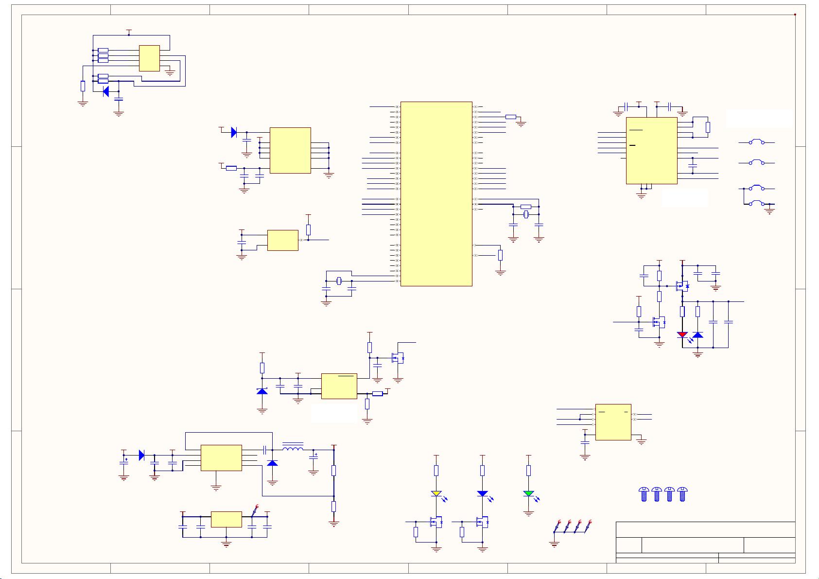
MAX31865
BIAS
REFIN+
DVDD
V
DD
GND1
GND2
DGND
REFIN-DRDY
ISENSORSDI
SCLK
HOST
INTERFACE
CS
SDO
N.C.
FORCE-
R
REF
RTD
R
CABLE
R
CABLE
0.1µF
V
DD
FORCE+
FORCE2
RTDIN+
RTDIN-
C
I
*
R
CABLE
R
CABLE
0.1µF
V
DD
4-WIRE SENSOR CONNECTION
*C
I
= 10nF FOR 1k RTD
100nF FOR 100 RTD
本文是英文数据资料的译文,文中可能存在翻译上的不准确或错误。如需进一步确认,请在您的设计中参考英文资料。
有关价格、供货及订购信息,请联络Maxim亚洲销售中心:108008521249(北中国区),108001521249(南中国区),
或访问Maxim的中文网站:www.maximintegrated.com/cn。
MAX31865
RTD至数字输出转换器
2
www.maximintegrated.com/cn
Voltage Range on V
DD
Relative to GND1 ............-0.3V to +4.0V
Voltage Range on BIAS, REFIN+,
REFIN-, ISENSOR ................................. -0.3V to (V
DD
+ 0.3V)
Voltage Range on FORCE+, FORCE2,
FORCE-, RTDIN+, RTDIN- Relative to GND1 ....-50V to +50V
Voltage Range on DVDD Relative to DGND ........-0.3V to +4.0V
Voltage Range on All Digital Pins
Relative to DGND ............................. -0.3V to (V
DVDD
+ 0.3V)
Continuous Power Dissipation (T
A
= +70NC)
TQFN (derate 34.5mW/NC above +70NC)...............2758.6mW
SSOP (derate 11.9mW/°C above +70° C)...............952.4mW
ESD Protection (all pins, Human Body Model) ...................±2kV
Operating Temperature Range ........................ -40NC to +125NC
Junction Temperature .....................................................+150NC
Storage Temperature Range ............................ -65NC to +150NC
Soldering Temperature (reflow) ......................................+260NC
Lead Temperature (soldering,10s) .................................+300NC
TQFN
Junction-to-Ambient Thermal Resistance (q
JA
) ..........29°C/W
Junction-to-Case Thermal Resistance (q
JC
) .................2°C/W
SSOP
Junction-to-Ambient Thermal Resistance (q
JA
) ..........84°C/W
Junction-to-Case Thermal Resistance (q
JC
) ...............32°C/W
Absolute Maximum Ratings
Note 1: Package thermal resistances were obtained using the method described in JEDEC specification JESD51-7, using a four-layer
board. For detailed information on package thermal considerations, refer to www.maximintegrated.com/thermal-tutorial.
Stresses beyond those listed under “Absolute Maximum Ratings” may cause permanent damage to the device. These are stress ratings only, and functional opera-
tion of the device at these or any other conditions beyond those indicated in the operational sections of the specifications is not implied. Exposure to absolute
maximum rating conditions for extended periods may affect device reliability.
Package Thermal Characteristics (Note 1)
Recommended DC Operating Conditions
(T
A
= -40NC to +125NC, unless otherwise noted.) (Notes 2 and 3)
Electrical Characteristics
(3.0V P V
DD
P 3.6V, T
A
= -40NC to +125NC, unless otherwise noted. Typical values are T
A
= +25NC, V
DD
= V
DVDD
= 3.3V.) (Notes 2
and 3)
MAX31865 RTD-to-Digital Converter
www.maximintegrated.com
Maxim Integrated
│
2
PARAMETER SYMBOL CONDITIONS MIN TYP MAX UNITS
V
DD
V
DD
3.0 3.3 3.6 V
DVDD V
DVDD
3.0 3.3 3.6 V
Input Logic 0 V
IL
CS, SDI, SCLK
-0.3
0.3 x
V
DVDD
V
Input Logic 1 V
IH
CS, SDI, SCLK
0.7 x
V
DVDD
V
DVDD
+ 0.3
V
Analog Voltages
(FORCE+,FORCE2, FORCE-,
RTDIN+, RTDIN-)
Normal conversion results 0 V
BIAS
V
Reference Resistor R
REF
350 10k
I
Cable Resistance R
CABLE
Per lead 0 50
I
PARAMETER SYMBOL CONDITIONS MIN TYP MAX UNITS
ADC Resolution No missing codes 15 Bits
ADC Full-Scale Input Voltage
(RTDIN+ - RTDIN-)
REFIN+ -
REFIN-
V

MAX31865
RTD至数字输出转换器
3
www.maximintegrated.com/cn
Electrical Characteristics (continued)
(3.0V P V
DD
P 3.6V, T
A
= -40NC to +125NC, unless otherwise noted. Typical values are T
A
= +25NC, V
DD
= V
DVDD
= 3.3V.) (Notes 2
and 3)
MAX31865 RTD-to-Digital Converter
www.maximintegrated.com
Maxim Integrated
│
3
PARAMETER SYMBOL CONDITIONS MIN TYP MAX UNITS
ADC Common-Mode Input
Range
0 V
BIAS
V
Input Leakage Current
RTDIN+, RTDIN-, 0NC to +70NC, on-state
2
nA
RTDIN+, RTDIN-, -40NC to +85NC, on-state
5
RTDIN+, RTDIN-, -40NC to 100NC, on-state
14
Bias Voltage V
BIAS
1.95 2.00 2.06 V
Bias Voltage Output Current I
OUT
0.2 5.75 mA
Bias Voltage Load Regulation
I
OUT
P 5.75mA
30 mV/mA
Bias Voltage Startup Time (Note 4) 10 ms
ADC Full-Scale Error
±1
LSB
ADC Integral Nonlinearity
Differential Input, endpoint fit, 0.3 x V
BIAS
P V
REF
P V
BIAS
±1
LSB
ADC Offset Error -3 +3 LSB
Noise (over Nyquist Bandwidth) Input referred 150
FV RMS
Common-Mode Rejection 90 dB
50/60Hz Noise Rejection Fundamental and harmonics 82 dB
Temperature Conversion Time
(Note 5)
t
CONV
Continuous conversion (60Hz notch) 16.7 17.6
ms
Single conversion (60Hz notch) 52 55
Single conversion (50Hz notch) 62.5 66
Continuous conversion (50Hz notch) 20 21
Automatic Fault Detection Cycle
Time
From CS high to cycle complete
550 600
Fs
Power-Supply Rejection 1 LSB/V
Power-Supply Current (Note 6)
I
DD
Shutdown
Bias off, ADC off 1.5 3 mA
I
DD
Bias on, active conversion 2 3.5 mA
Power-On Reset Voltage
Threshold
2 2.27 V
Power-On Reset Voltage
Hysteresis
120 mV
Input Capacitance C
IN
Logic inputs 6 pF
Input Leakage Current I
L
Logic inputs -1 +1
FA
Output High Voltage V
OH
I
OUT
= -1.6mA
V
DVDD
- 0.4
V
Output Low Voltage V
OL
I
OUT
= 1.6mA 0.4 V

MAX31865
RTD至数字输出转换器
4
www.maximintegrated.com/cn
Note 2: All voltages are referenced to ground when common. Currents entering the IC are specified positive.
Note 3: Limits are 100% production tested at T
A
= +25°C and/or T
A
= +85°C. Limits over the operating temperature range and rel-
evant supply voltage range are guaranteed by design and characterization. Typical values are not guaranteed.
Note 4: For 15-bit settling, a wait of at least 10.5 time constants of the input RC network is required. Max startup time is calculated
with a 10kω reference resistor and a 0.1µF capacitor across the RTD inputs.
Note 5: The first conversion after enabling continuous conversion mode takes a time equal to the single conversion time for the
respective notch frequency.
Note 6: Specified with no load on the bias pin as the sum of analog and digital currents. No active communication. If the RTD
input voltage is greater than the input reference voltage, then an additional 400µA I
DD
can be expected.
Note 7: All timing specifications are guaranteed by design.
Note 8: Measured at V
IH
= 0.7V x V
DVDD
or V
IL
= 0.3 x V
DVDD
and 10ms maximum rise and fall times.
Note 9: Measured with 50pF load.
Note 10: Measured at V
OH
= 0.7 x V
DVDD
or V
OL
= 0.3 x V
DVDD
. Measured from the 50% point of SCLK to the V
OH
minimum of
SDO.
AC Electrical Characteristics: SPI Interface
(3.0V P V
DD
P 3.6V, T
A
= -40NC to +125NC, unless otherwise noted. Typical values are T
A
= +25NC, V
DD
= V
DVDD
= 3.3V.) (Notes 3
and 7) (Figure 1 and Figure 2)
MAX31865 RTD-to-Digital Converter
www.maximintegrated.com
Maxim Integrated
│
4
PARAMETER SYMBOL CONDITIONS MIN TYP MAX UNITS
Data to SCLK Setup t
DC
(Notes 8, 9) 35 ns
SCLK to Data Hold t
CDH
(Notes 8, 9) 35 ns
SCLK to Data Valid t
CDD
(Notes 8, 9, 10) 80 ns
SCLK Low Time t
CL
(Note 9) 100 ns
SCLK High Time t
CH
(Note 9) 100 ns
SCLK Frequency t
CLK
(Note 9) DC 5.0 MHz
SCLK Rise and Fall t
R
, t
F
(Note 9) 200 ns
CS to SCLK Setup
t
CC
(Note 9) 400 ns
SCLK to CS Hold
t
CCH
(Note 9) 100 ns
CS Inactive Time
t
CWH
(Note 9) 400 ns
CS to Output High-Z
t
CDZ
(Notes 8, 9) 40 ns
Address 01h or 02h Decoded to
DRDY High
t
DRDYH
After RTD register read access (Note 9) 50 ns
MAX31865
RTD至数字输出转换器
5
www.maximintegrated.com/cn
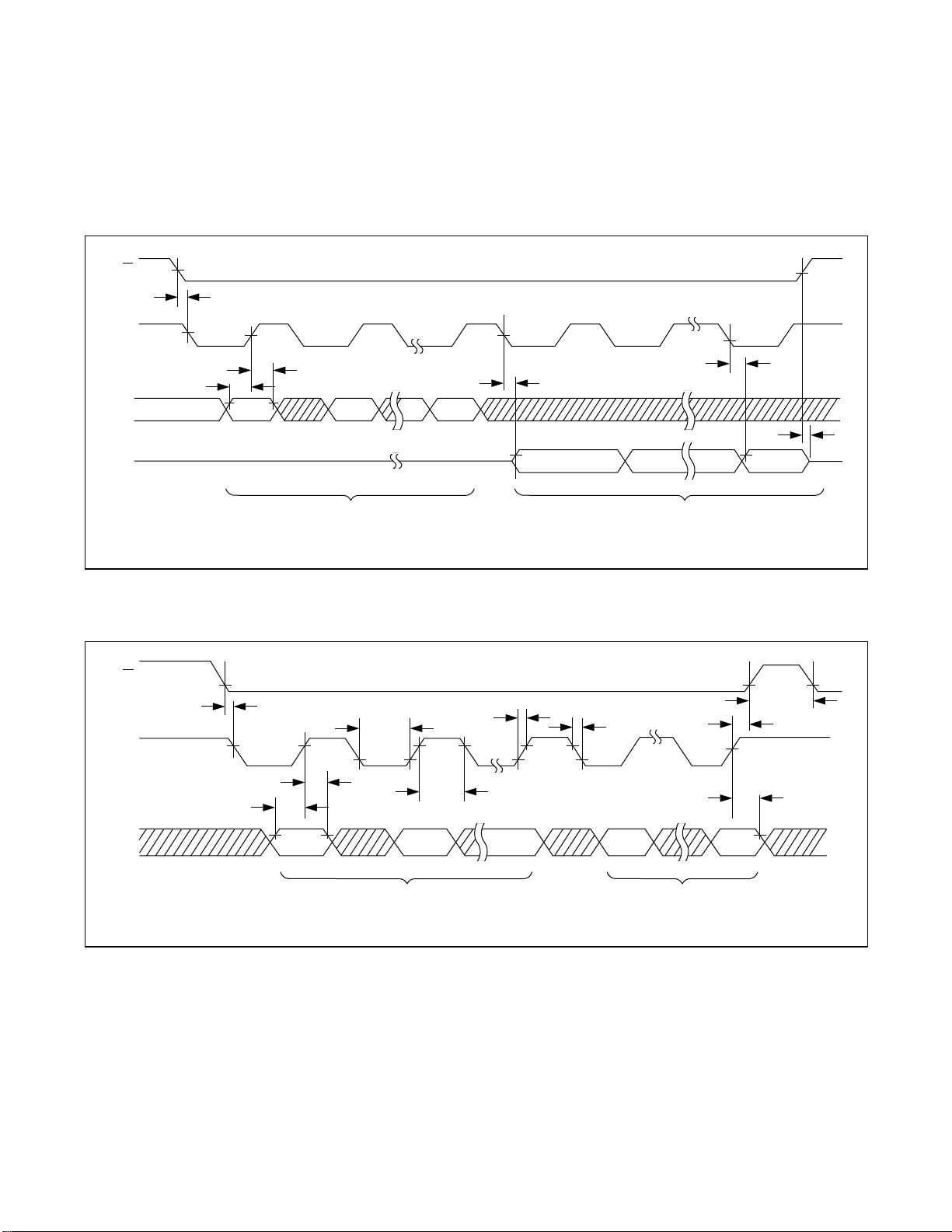
Figure 1. Timing Diagram: SPI Read Data Transfer
Figure 2. Timing Diagram: SPI Write Data Transfer
MAX31865 RTD-to-Digital Converter
www.maximintegrated.com
Maxim Integrated
│
5
CS
SCLK
SDI
SDO
t
CC
t
CDH
A7 A6 A0
D7 D6 D1 D0
t
DC
t
CDD
t
CDD
t
CDZ
NOTE: SCLK CAN BE EITHER POLARITY, TIMING SHOWN FOR CPOL = 1.
WRITE ADDRESS BYTE READ DATA BYTE
SCLK
SDI
NOTE: SCLK CAN BE EITHER POLARITY, TIMING SHOWN FOR CPOL = 1.
WRITE ADDRESS BYTE WRITE DATA BYTE
t
CC
t
CDH
t
CH
t
R
t
F
t
CCH
t
CWH
t
CDH
A7 A6 A0 D7 D0
t
DC
t
CL
CS
图1. 时序图:SPI读数据传输
图2. 时序图:SPI写数据传输


