没有合适的资源?快使用搜索试试~ 我知道了~
AD7190文档说明The AD7190 is a low noise, complete analog front end for high precision measurement applications. It contains a low noise, 24-bit sigma-delta (Σ-Δ) analog-to-digital converter (ADC). The on-chip low noise gain stage means that signals of small amplitude can be interfaced directly to the ADC.
资源推荐
资源详情
资源评论


4.8 kHz Ultralow Noise 24-Bit
Sigma-Delta ADC with PGA
AD7190
Rev. B
Information furnished by Analog Devices is believed to be accurate and reliable. However, no
responsibility is assumed by Analog Devices for its use, nor for any infringements of patents or other
rights of third parties that may result from its use. Specifications subject to change without notice. No
license is granted by implication or otherwise under any patent or patent rights of Analog Devices.
Trademarks and registered trademarks are the property of their respective owners.
One Technology Way, P.O. Box 9106, Norwood, MA 02062-9106, U.S.A.
Tel: 781.329.4700 www.analog.com
Fax: 781.461.3113 ©2008–2009 Analog Devices, Inc. All rights reserved.
FEATURES
RMS noise: 8.5 nV @ 4.7 Hz (gain = 128)
16 noise free bits @ 2.4 kHz (gain = 128)
Up to 22.5 noise free bits (gain = 1)
Offset drift: 5 nV/°C
Gain drift: 1 ppm/°C
Specified drift over time
2 differential/4 pseudo differential input channels
Automatic channel sequencer
Programmable gain (1 to 128)
Output data rate: 4.7 Hz to 4.8 kHz
Internal or external clock
Simultaneous 50 Hz/60 Hz rejection
4 general-purpose digital outputs
Power supply
AV
DD
: 4.75 V to 5.25 V
DV
DD
: 2.7 V to 5.25 V
Current: 6 mA
Temperature range: –40°C to +105°C
Interface
3-wire serial
SPI, QSPI™, MICROWIRE™, and DSP compatible
Schmitt trigger on SCLK
APPLICATIONS
Weigh scales
Strain gauge transducers
Pressure measurement
Temperature measurement
Chromatography
PLC/DCS analog input modules
Data acquisition
Medical and scientific instrumentation
GENERAL DESCRIPTION
The AD7190 is a low noise, complete analog front end for high
precision measurement applications. It contains a low noise,
24-bit sigma-delta (∑-Δ) analog-to-digital converter (ADC).
The on-chip low noise gain stage means that signals of small
amplitude can be interfaced directly to the ADC.
The device can be configured to have two differential inputs or
four pseudo differential inputs. The on-chip channel sequencer
allows several channels to be enabled, and the AD7190
sequentially converts on each enabled channel. This simplifies
communication with the part. The on-chip 4.92 MHz clock can
be used as the clock source to the ADC or, alternatively, an
external clock or crystal can be used. The output data rate from
the part can be varied from 4.7 Hz to 4.8 kHz.
The device has two digital filter options. The choice of filter
affects the rms noise/noise-free resolution at the programmed
output data rate, the settling time, and the 50 Hz/60 Hz
rejection. For applications that require all conversions to be
settled, the AD7190 includes a zero latency feature.
The part operates with 5 V analog power supply and a digital
power supply from 2.7 V to 5.25 V. It consumes a current of
6 mA. It is housed in a 24-lead TSSOP package.
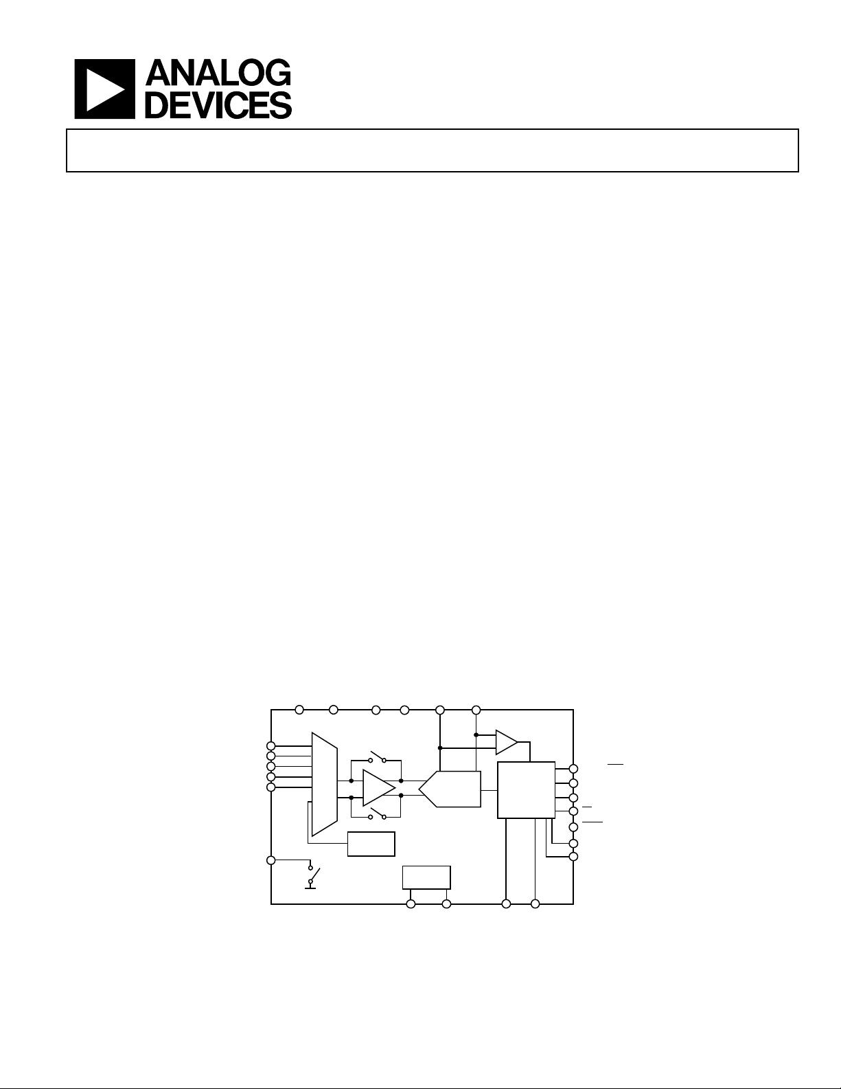
FUNCTIONAL BLOCK DIAGRAM
MCLK1 MCLK2 P0/REFIN2(–) P1/REFIN2(+)
DV
DD
DGND REFIN1(+) REFIN1(–)
AIN1
AIN2
AIN3
AIN4
A
INCOM
BPDSW
AGND
AD7190
REFERENCE
DETECT
SERIAL
INTERFACE
AND
CONTROL
LOGIC
TEMP
SENSOR
CLOCK
CIRCUITRY
DOUT/RDY
DIN
SCLK
CS
SYNC
P3
P2
AV
DD
AGND
Σ-Δ
ADC
PGA
MUX
07640-001
Figure 1.

AD7190
Rev. B | Page 2 of 40
TABLE OF CONTENTS
Features .............................................................................................. 1
Applications ....................................................................................... 1
General Description ......................................................................... 1
Functional Block Diagram .............................................................. 1
Revision History ............................................................................... 2
Specifications ..................................................................................... 3
Timing Characteristics ................................................................ 7
Circuit and Timing Diagrams ..................................................... 7
Absolute Maximum Ratings ............................................................ 9
Thermal Resistance ...................................................................... 9
ESD Caution .................................................................................. 9
Pin Configuration and Function Descriptions ........................... 10
Typical Performance Characteristics ........................................... 12
RMS Noise and Resolution ............................................................ 15
Sinc
4
Chop Disabled ................................................................... 15
Sinc
3
Chop Disabled ................................................................... 16
Sinc
4
Chop Enabled .................................................................... 17
Sinc
3
Chop Enabled .................................................................... 18
On-Chip Registers .......................................................................... 19
Communications Register ......................................................... 19
Status Register ............................................................................. 20
Mode Register ............................................................................. 20
Configuration Register .............................................................. 22
Data Register ............................................................................... 24
ID Register ................................................................................... 24
GPOCON Register ..................................................................... 24
Offset Register ............................................................................. 25
Full-Scale Register ...................................................................... 25
ADC Circuit Information .............................................................. 26
Overview ..................................................................................... 26
Filter, Output Data Rate, Settling Time ................................... 26
Digital Interface .......................................................................... 29
Circuit Description......................................................................... 33
Analog Input Channel ............................................................... 33
PGA .............................................................................................. 33
Bipolar/Unipolar Configuration .............................................. 33
Data Output Coding .................................................................. 33
Clock ............................................................................................ 33
Burnout Currents ....................................................................... 34
Reference ..................................................................................... 34
Reference Detect ......................................................................... 34
Reset ............................................................................................. 34
System Synchronization ............................................................ 35
Temperature Sensor ................................................................... 35
Bridge Power-Down Switch ...................................................... 35
Logic Outputs ............................................................................. 35
Enable Parity ............................................................................... 36
Calibration ................................................................................... 36
Grounding and Layout .............................................................. 37
Applications Information .............................................................. 38
Weigh Scales ................................................................................ 38
Outline Dimensions ....................................................................... 39
Ordering Guide .......................................................................... 39
REVISION HISTORY
5/09—Rev. A to Rev. B
Changes to Table 3 ............................................................................ 9
5/09—Rev. 0 to Rev. A
Changes to Table 1 ............................................................................ 3
Changes to Table 3 and Table 4 ....................................................... 9
Changes to Table 5 .......................................................................... 10
Changes to Table 6 and Table 7 ..................................................... 15
Changes to Status Register Section .............................................. 20
Changes to Table 17 ........................................................................ 21
Changes to Table 19 ........................................................................ 23
Changes to Table 20 ........................................................................ 24
Added ID Register Section ............................................................ 24
Changes to Table 21 ....................................................................... 25
Changes to Filter, Output Data Rate, Settling Time Section .... 26
Changes to Continuous Conversion Mode Section ................... 31
Changes to Analog Input Channel and Bipolar/Unipolar
Configuration Sections .................................................................. 33
Changes to Burnout Currents, Reference, Reference Detect, and
Reset Sections .................................................................................. 34
Changes to Temperature Sensor Section ..................................... 35
Changes to Calibration Section .................................................... 36
Changes to Grounding and Layout Section ................................ 37
Changes to Weigh Scales Section ................................................. 38
Changes to Ordering Guide .......................................................... 39
10/08—Revision 0—Initial Version

AD7190
Rev. B | Page 3 of 40
SPECIFICATIONS
AV
DD
= 4.75 V to 5.25 V, DV
DD
= 2.7 V to 5.25 V, AGND = DGND = 0 V, REFINx(+) = AV
DD
, REFINx(−) = AGND, MCLK = 4.92 MHz,
T
A
= T
MIN
to T
MAX
, unless otherwise noted.
Table 1.
Parameter AD7190B Unit Test Conditions/Comments
1
ADC
Output Data Rate 4.7 to 4800 Hz nom Chop disabled.
1.17 to 1200 Hz nom Chop enabled, sinc
4
filter.
1.56 to 1600 Hz nom Chop enabled, sinc
3
filter.
No Missing Codes
2
24 Bits min FS > 1, sinc
4
filter
3
.
24 Bits min FS > 4, sinc
3
filter
3
.
Resolution
See the RMS Noise and
Resolution section
RMS Noise and Output Data Rates
See the RMS Noise and
Resolution section
Integral Nonlinearity ±5 ppm of FSR max ±1 ppm typical, gain = 1.
±15 ppm of FSR max ±5 ppm typical, gain > 1.
Offset Error
4, 5
±75/gain μV typ Chop disabled.
±0.5 μV typ Chop enabled.
Offset Error Drift vs. Temperature
5
±100/gain nV/°C typ Gain = 1 to 16. chop disabled.
±5 nV/°C typ Gain = 32 to 128. chop disabled.
±5 nV/°C typ Chop enabled.
Offset Error Drift vs. Time 25 nV/1000 hours typ Gain ≥ 32.
Gain Error
4
±0.005 % max ±0.001 % typical, gain = 1, AV
DD
= 5 V
6
.
±0.0075 % typ Gain > 1, post internal full-scale calibration.
Gain Drift vs. Temperature ±1 ppm/°C typ
Gain Drift vs. Time 10 ppm/1000 hours typ Gain = 1.
Power Supply Rejection 95 dB typ Gain = 1, V
IN
= 1 V.
100 dB min Gain > 1, V
IN
= 1 V/gain. 110 dB typical.
Common-Mode Rejection
@ DC 100 dB min Gain = 1, V
IN
= 1 V
2
.
110 dB min Gain > 1, V
IN
= 1 V/gain.
@ 50 Hz, 60 Hz
2
120 dB min 10 Hz output data rate, 50 ± 1 Hz, 60 ± 1 Hz.
@ 50 Hz, 60 Hz
2
120 dB min
50 ± 1 Hz (50 Hz output data rate), 60 ± 1 Hz
(60 Hz output data rate).
Normal Mode Rejection
2
Sinc
4
Filter
Internal Clock
@ 50 Hz, 60 Hz 100 dB min 10 Hz output data rate, 50 ± 1 Hz, 60 ± 1 Hz.
74 dB min
50 Hz output data rate, REJ60
7
= 1,
50 ± 1 Hz, 60 ± 1 Hz.
@ 50 Hz 96 dB min 50 Hz output data rate, 50 ± 1 Hz.
@ 60 Hz 97 dB min 60 Hz output data rate, 60 ± 1 Hz.

AD7190
Rev. B | Page 4 of 40
Parameter AD7190B Unit Test Conditions/Comments
1
External Clock
@ 50 Hz, 60 Hz 120 dB min 10 Hz output data rate, 50 ± 1 Hz, 60 ± 1 Hz.
82 dB min
50 Hz output data rate, REJ60
7
= 1,
50 ± 1 Hz, 60 ± 1 Hz.
@ 50 Hz 120 dB min 50 Hz output data rate, 50 ± 1 Hz.
@ 60 Hz 120 dB min 60 Hz output data rate, 60 ± 1 Hz.
Sinc
3
Filter
Internal Clock
@ 50 Hz, 60 Hz 75 dB min 10 Hz output data rate, 50 ± 1 Hz, 60 ± 1 Hz.
60 dB min
50 Hz output data rate, REJ60 = 1,
50 ± 1 Hz, 60 ± 1 Hz.
@ 50 Hz 70 dB min 50 Hz output data rate, 50 ± 1 Hz.
@ 60 Hz 70 dB min 60 Hz output data rate, 60 ± 1 Hz.
External Clock
@ 50 Hz, 60 Hz 100 dB min 10 Hz output data rate, 50 ± 1 Hz, 60 ± 1 Hz.
67 dB min
50 Hz output data rate, REJ60
7
= 1,
50 ± 1 Hz, 60 ± 1 Hz.
@ 50 Hz 95 dB min 50 Hz output data rate, 50 ± 1 Hz.
@ 60 Hz 95 dB min 60 Hz output data rate, 60 ± 1 Hz.
ANALOG INPUTS
Differential Input Voltage Ranges ±V
REF
/gain V nom
V
REF
= REFINx(+) − REFINx(−),
gain = 1 to 128.
±(AV
DD
– 1.25 V)/gain V min/max Gain > 1.
Absolute AIN Voltage Limits
2
Unbuffered Mode AGND − 50 mV V min
AV
DD
+ 50 mV V max
Buffered Mode AGND + 250 mV V min
AV
DD
− 250 mV V max
Analog Input Current
Buffered Mode
Input Current
2
±2 nA max Gain = 1.
±3 nA max Gain > 1.
Input Current Drift ±5 pA/°C typ
Unbuffered Mode
Input Current ±5 μA/V typ
Gain = 1, input current varies with input
voltage.
±1 μA/V typ Gain > 1.
Input Current Drift ±0.05 nA/V/°C typ External clock.
±1.6 nA/V/°C typ Internal clock.
REFERENCE INPUT
REFIN Voltage AV
DD
V nom REFIN = REFINx(+) − REFINx(−).
Reference Voltage Range
2
1 V min
AV
DD
V max
The differential input must be limited to
± (AV
DD
– 1.25 V)/gain when gain > 1.
Absolute REFIN Voltage Limits
2
AGND – 50 mV V min
AV
DD
+ 50 mV V max
Average Reference Input Current 7 μA/V typ
Average Reference Input Current
Drift
±0.03 nA/V/°C typ External clock.
1.3 nA/V/°C typ Internal clock.

AD7190
Rev. B | Page 5 of 40
Parameter AD7190B Unit Test Conditions/Comments
1
Normal Mode Rejection
2
Same as for analog inputs
Common-Mode Rejection 95 dB typ
Reference Detect Levels 0.3 V min
0.6 V max
TEMPERATURE SENSOR
Accuracy ±2 °C typ Applies after user calibration at 25°C.
Sensitivity 2815 Codes/°C typ Bipolar mode.
BRIDGE POWER-DOWN SWITCH
R
ON
10 Ω max
Allowable Current
2
30 mA max Continuous current.
BURNOUT CURRENTS
AIN Current 500 nA nom
Analog inputs must be buffered and chop
disabled.
DIGITAL OUTPUTS (P0 to P3)
Output High Voltage, V
OH
2
4 V min AV
DD
= 5V, I
SOURCE
= 200 μA.
Output Low Voltage, V
OL
2
0.4 V max AV
DD
= 5V, I
SINK
= 800 μA.
Floating-State Leakage Current ±100 nA max
Floating-State Output
Capacitance
10 pF typ
INTERNAL/EXTERNAL CLOCK
Internal Clock
Frequency 4.92 ± 4% MHz min/max
Duty Cycle 50:50 % typ
External Clock/Crystal
2
Frequency 4.9152 MHz nom
2.4576/5.12 MHz min/max
Input Low Voltage, V
INL
0.8 V max DV
DD
= 5 V.
0.4 V max DV
DD
= 3 V.
Input High Voltage, V
INH
2.5 V min DV
DD
= 3 V.
3.5 V min DV
DD
= 5 V.
Input Current ±10 μA max
LOGIC INPUTS
Input High Voltage, V
INH
2
2 V min
Input Low Voltage, V
INL
2
0.8 V max
Hysteresis
2
0.1/0.25 V min/V max
Input Currents ±10 μA max
LOGIC OUTPUT (DOUT/RDY)
Output High Voltage, V
OH
2
DV
DD
− 0.6 V min DV
DD
= 3 V, I
SOURCE
= 100 μA.
Output Low Voltage, V
OL
2
0.4 V max DV
DD
= 3 V, I
SINK
= 100 μA.
Output High Voltage, V
OH
2
4 V min DV
DD
= 5 V, I
SOURCE
= 200 μA.
Output Low Voltage, V
OL
2
0.4 V max DV
DD
= 5 V, I
SINK
= 1.6 mA.
Floating-State Leakage Current ±10 μA max
Floating-State Output
Capacitance
10 pF typ
Data Output Coding Offset binary
SYSTEM CALIBRATION
2
Full-Scale Calibration Limit 1.05 × FS V max
Zero-Scale Calibration Limit −1.05 × FS V min
Input Span 0.8 × FS V min
2.1 × FS V max
剩余39页未读,继续阅读
资源评论


FeiYing_1102
- 粉丝: 0
- 资源: 2
上传资源 快速赚钱
我的内容管理 展开
我的资源 快来上传第一个资源
我的收益
登录查看自己的收益我的积分 登录查看自己的积分
我的C币 登录后查看C币余额
我的收藏
我的下载
下载帮助


最新资源
- ASL6328芯片规格说明书
- 基于Matlab实现智能体一阶有领导者仿真(源码+数据).rar
- 独立公众号版本微信社群人脉系统社群空间站最新源码+详细教程
- 森林图像数据集(2700张图片).rar
- 《基于Comsol仿真模拟的岩石损伤研究-水力压裂实验探究》,利用Comsol仿真模拟技术精确预测水力压裂过程中岩石损伤情况,comsol仿真模拟水力压裂岩石损伤 ,关键词:COMSOL仿真;水
- 自由方舟管理后台通用模板-基于TDesign二次优化
- 《学习CRUISE M热管理的视频教程及文档解说,无需模型,轻松入门》,CRUISE M热管理视频教程:无模型,文档解说,轻松学习掌握热管理知识,录的CRUISE M热管理视频,有文档解说,没有模型
- 洛杉矶犯罪数据集概览 (2020年至今),犯罪事件数据集,犯罪影响因素
- 电信客户流失数据集,运营商流失客户数据集
- FinalBurn Neo源代码
- 基于积分型滑模控制器的永磁同步电机FOC转速环设计及仿真模型参考,基于积分型滑模控制器的永磁同步电机FOC转速环设计及仿真模型参考,基于积分型滑模控制器的永磁同步电机FOC 1.转速环基于积分型滑模面
- 智能车辆模拟系统:深度探究多步泊车,平行泊车与垂直泊车的仿真应用,《深入探讨carsim仿真技术下的多步泊车策略:平行泊车与垂直泊车的实现与优化》,carsim仿真多步泊车,平行泊车和垂直泊车 ,核心
- BMS模块Simulink开发基于算法,基于Simulink开发的BMS算法:包含SOC计算、故障处理与状态监测的充放电控制策略图解,BMS Simulink 所有算法基于Simulink开发 BMS
- 犯罪率与社会经济因素数据集,探讨了犯罪率与各种社会经济因素之间的关系,如教育水平、就业率、中位收入、贫困率和人口密度涵盖了1000个地区的数据
- ASL6328芯片原理图-V1.1
- 精品源码Javaweb仓库管理系统项目源码
资源上传下载、课程学习等过程中有任何疑问或建议,欢迎提出宝贵意见哦~我们会及时处理!
点击此处反馈


安全验证
文档复制为VIP权益,开通VIP直接复制
